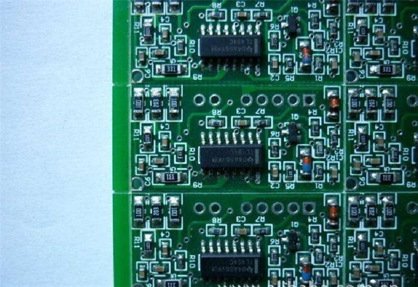
Sputtering targets have important applications in many areas, such as architecture, optics, electronics and so on. Sputtering targets used in electronic industry can be subdivided into semiconductor target (also called anelva target), planar target, coated glass target, solar photovoltaic target, and so on. There are some differences in the selection and performance requirements of sputtering materials in different application fields. Among them, anelva targets, the sputtering targets used in semiconductor integrated circuits, are the most demanding and strict.
The table below shows the main types, uses, and performance requirements for sputtering targets in the electronics field. If it helps you, please share this article with your friends.
| Type | Application | Main Variety | Performance Requirements |
| Semiconductor | Used to prepare integrated circuit core materials | W, WTi, Ti, Ta, Al alloy with purity 4N or 5N. | Highest technical requirements; ultra-high purity metal; high precision size; high integration |
| Flat display | Sputtering technology guarantees uniformity of film produced, increases productivity and reduces costs | Nb, Si, Cr, Mo, MoNb, Al alloy , Cu and Cu alloy targets | High technical requirements; high purity materials; large material area; high uniformity |
| Decoration | Used for coating the surface of the product for beautification, wear resistance and corrosion resistance. | Cr, Ti, Zr, Ni, W, TiAl, CrSi, CrTi, CrAlZr target | General technical requirements; mainly used for decoration, energy-saving, etc. |
| Tool | Enhance the surface of tools and molds, improve the life and the quality of the parts manufactured | TiAl, CrAl, Cr, Ti, TiC, Al2O3 target | High-performance requirements; extended service life |
| Solar | Sputter coating technology for the production of fourth-generation thin-film solar cells | ZnOAl, ZnO, ZnAl, Mo, CdS, CIGS target | High technical requirements; large application range |
| Electron device | Thin-film resistors, film capacitors | NiCr, NiCrSi, CrSi, Ta, NiCrAl target | Requires small size, good stability, and low-temperature coefficient of resistance |
| Information storage | Used to make storage | Cr alloy, Co alloy, CoFe alloy, Ni alloy | High storage density; high transmission speed |


