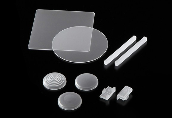
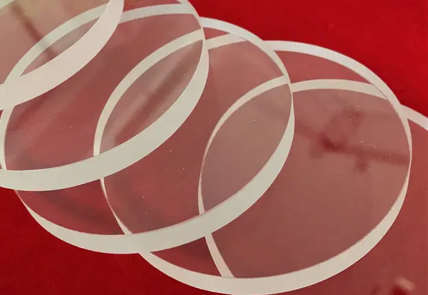
Introduction
In the realm of semiconductor manufacturing, the choice of substrate material is critical, directly impacting the performance and durability of the end product. Semiconductor substrates serve as the foundational layer for the deposition of various electronic circuits, and their material properties can significantly influence the efficiency and functionality of these devices. Among the various substrates used, sapphire has been widely favored for its durability and cost-effectiveness. However, the advent of Chemical Vapor Deposition (CVD) diamond wafers is beginning to challenge this standard due to their outstanding attributes. This article explores the potential shift towards CVD diamond wafers, examining their superior qualities compared to traditional sapphire substrates and delineating their role in pushing the boundaries of semiconductor technology.
Comparison of CVD Diamond and Sapphire
Physical Properties
One of the most significant advantages of CVD diamond wafers over sapphire substrates lies in their physical properties. Diamond, renowned as the hardest material known, offers exceptional resistance to wear and abrasion, which is critical for high-durability applications. Moreover, its thermal conductivity is unmatched, reaching up to 2200 W/mK, compared to sapphire’s modest 35 W/mK. This superior thermal performance means that CVD diamond wafers can handle much higher thermal loads, effectively dissipating heat and thus mitigating thermal stress in semiconductor devices. This capability is particularly beneficial in high-power and high-frequency electronic applications where heat accumulation could otherwise lead to device failure.
Electrical Properties
Electrically, CVD diamond wafers exhibit outstanding properties that enhance device performance. They feature a high carrier mobility, which allows for faster electron movement within the semiconductor, crucial for high-speed electronics. Additionally, diamond’s low dielectric constant minimizes power losses during electronic operations, thereby enhancing overall device efficiency. These properties make CVD diamond particularly advantageous for applications that require high power density and operational frequency, where sapphire substrates might not perform as well due to their relatively lower electrical efficiencies.
Optical Properties
From an optical perspective, CVD diamond wafers are transparent across a wide range of wavelengths, from ultraviolet (UV) to far-infrared, providing an essential advantage for optoelectronic devices, such as sensors and laser systems. This broad transparency spectrum enables versatile applications in various fields, including telecommunications and medical devices. In contrast, while sapphire also shows good transparency from the UV to the near-infrared spectrum, it does not efficiently cover the far-infrared range, thus limiting its utility in applications requiring broader wavelength transparency.
Advantages of CVD Diamond Wafers
The distinct physical, electrical, and optical properties of CVD diamond wafers translate into significant advantages in semiconductor applications. These benefits are pivotal for industries demanding extreme performance and reliability.
Superior Thermal Management: The exceptional thermal conductivity of diamond plays a critical role in managing heat effectively in semiconductor devices. This ability to rapidly dissipate heat not only enhances the performance but also significantly extends the lifespan of devices by preventing thermal degradation. This is especially advantageous in high-power electronics and devices operating under high thermal loads, where sapphire substrates might falter.
Enhanced Electrical Performance: The high carrier mobility and low dielectric constant of diamond contribute to reduced power losses and higher operational speeds. Devices built on diamond substrates can achieve greater efficiency and faster response times, critical for advanced computing and high-frequency RF applications. This makes CVD diamond an ideal choice for next-generation semiconductor devices where performance cannot be compromised.
Increased Device Durability: The unmatched hardness and robustness of diamond also contribute to the increased durability of semiconductor devices. Diamond substrates are less susceptible to wear and damage during manufacturing and operation, which translates into lower maintenance costs and longer device lifecycles. This durability is particularly valuable in military and aerospace applications, where reliability and longevity are paramount.
Eco-friendly Material: Beyond performance metrics, diamond is also considered a more environmentally friendly option compared to other substrate materials. Its ability to operate efficiently at higher temperatures reduces energy consumption and the carbon footprint of manufacturing processes.
Challenges and Limitations
Despite their superior properties and potential benefits, CVD diamond wafers are not without challenges and limitations, which currently restrict their widespread adoption in the semiconductor industry.
Production Complexity: The synthesis of high-quality CVD diamond involves complex chemical processes under highly controlled conditions, which can be both time-consuming and costly. The deposition process requires specialized equipment and precise control of temperature, pressure, and gas mixtures, which not all manufacturing facilities can support. This complexity contributes to higher production costs compared to simpler processes used for sapphire substrates.
Cost Factors: Initially, the cost of producing CVD diamond wafers is significantly higher than that of sapphire. The raw materials, energy requirements, and intricate manufacturing processes make diamond substrates more expensive. This cost factor is a considerable barrier, especially for applications where cost-effectiveness is as critical as performance.
Scalability Issues: Scaling the production of CVD diamond to meet large volume demands while maintaining quality remains a significant challenge. While advancements are being made, the ability to produce large quantities of uniform quality diamond wafers is not yet at the level of more established materials like silicon or sapphire. This limitation affects the feasibility of using CVD diamond in mainstream semiconductor applications.
Limited Industry Experience: The semiconductor industry has extensive experience and established infrastructure for working with materials like silicon and sapphire. The shift to diamond substrates requires new expertise and adaptation of existing equipment and processes, which can slow down adoption and integration.
Applications and Future Potential
The unique attributes of CVD diamond wafers not only make them suitable for current high-end applications but also open doors to future innovations in various fields. Here are some of the most promising areas for their application:
High-Power Electronics: CVD diamond’s exceptional thermal conductivity and electrical properties make it ideal for use in high-power electronic devices, such as power amplifiers and switches, where heat dissipation is critical to maintaining functionality and reliability. This is particularly relevant in industries such as automotive and aerospace, where devices must perform under extreme conditions.
Optoelectronics and Photonics: The broad optical transparency of diamond across a wide range of wavelengths enhances its suitability for optoelectronic components like lasers, LEDs, and UV light sensors. These applications benefit from diamond’s ability to handle high energy densities without degrading, a critical requirement for advanced optical systems.
Quantum Computing: Diamond substrates are finding roles in the burgeoning field of quantum computing, particularly in the development of quantum bits (qubits) that can operate at room temperature. The nitrogen-vacancy centers in diamond provide a stable environment for these qubits, enabling more practical and scalable quantum computers.
RF Communications: In radio frequency applications, the high thermal and electrical conductivity of diamond helps in managing the thermal loads in RF amplifiers and antennas, improving signal integrity and performance in communication devices.
Future Growth Areas: Continued advancements in CVD technology and reduction in production costs are expected to enhance the adoption of diamond substrates in mainstream semiconductor manufacturing. As the technology matures, it is anticipated that new uses for CVD diamond will emerge, potentially transforming sectors like renewable energy, military defense systems, and more.
Conclusion
The exploration of CVD diamond wafers in the context of semiconductor substrates has illuminated their compelling advantages over traditional materials like sapphire. With unparalleled thermal and electrical properties, along with superior optical characteristics, CVD diamond stands out as a material that can significantly enhance the performance and durability of semiconductor devices. Despite facing challenges such as high production costs and complex manufacturing requirements, the potential applications and future prospects of CVD diamond make it a highly promising candidate for redefining the standards in semiconductor technology.
As the industry continues to evolve and technology advances, the barriers currently hindering the widespread adoption of CVD diamond are likely to diminish. With ongoing research and development aimed at overcoming these challenges, it is conceivable that CVD diamond will increasingly become a mainstream choice for semiconductor substrates. The adoption of CVD diamond could not only lead to higher-performing electronic devices but also open new avenues for innovation in fields ranging from high-power electronics to quantum computing.
In conclusion, while the transition to CVD diamond wafers represents a significant shift, the advantages they offer suggest a bright future where they could potentially set new benchmarks for performance and efficiency in semiconductor technologies.


