1. Introduction
Hexagonal boron nitride (hBN) thin films have garnered attention in advanced material applications due to their exceptional thermal stability, high electrical insulation, and chemical inertness. Structurally similar to graphene but electrically insulating, hBN thin films have become essential in fields requiring high-performance coatings, including aerospace, industrial tooling, and electronics.

This article explores the PVD processes used to deposit hBN thin films, highlighting their unique properties, technical advantages, and applications in high-performance coatings. By understanding the potential of PVD and hBN, industries can leverage this combination to meet the demands of modern engineering challenges.
2. The Unique Properties of hBN Thin Films
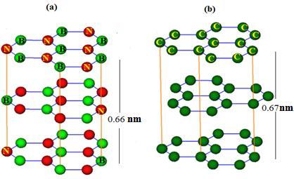
Hexagonal boron nitride (hBN) thin films are prized for their distinctive thermal, electrical, and chemical properties, making them versatile in advanced coating applications. These properties are directly linked to hBN’s unique hexagonal lattice structure, alternating boron and nitrogen atoms.
- Thermal Stability and Conductivity: hBN thin films exhibit exceptional thermal stability, withstanding temperatures exceeding 900°C in inert atmospheres. Their high thermal conductivity ensures efficient heat dissipation, making them ideal for applications like thermal management coatings in electronics and high-power LEDs.
- Electrical Insulation: hBN is an electrical insulator with a wide bandgap (~5.9 eV), which provides excellent dielectric properties. These characteristics are critical in electronic components, where hBN thin films act as protective layers, reducing energy loss and preventing short circuits in high-frequency devices.
- Chemical Inertness: hBN films demonstrate superior resistance to chemical attack, even in corrosive environments. This makes them suitable for protective coatings in industrial and aerospace applications, where exposure to harsh chemicals and extreme conditions is common.
- Mechanical Strength: The layered structure of hBN offers both strength and flexibility. This dual capability enables its integration into rigid systems and flexible electronics, where it provides mechanical support and stress resistance.
3. PVD Techniques for Depositing hBN Thin Films
Physical vapor deposition (PVD) methods are among the most effective approaches for depositing hexagonal boron nitride (hBN) thin films. PVD techniques offer unmatched precision, enabling the formation of high-purity, uniform thin films with customizable thicknesses. These methods are especially suited for applications requiring robust and high-performance coatings, such as aerospace components, industrial tools, and electronic devices.
Magnetron Sputtering
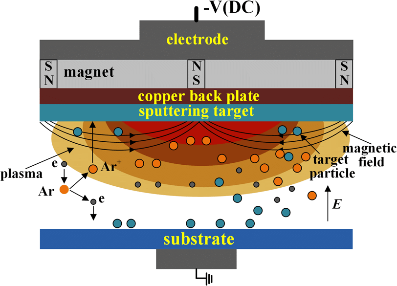
Magnetron sputtering is a widely used PVD method for depositing hBN thin films. In this process, a high-purity hBN sputtering target is bombarded by a plasma of inert gas ions (commonly argon), causing the ejection of hBN material, which then deposits onto the substrate. Key advantages of this technique include:
- Uniform Coatings: Magnetron sputtering ensures consistent thickness across large substrate areas, critical for applications like optical coatings and electronic insulation layers.
- Precision Control: Adjustable parameters, such as ion energy and gas flow, allow fine-tuning of film properties, including density and adhesion.
- Scalability: This method supports both research-scale experiments and industrial-scale production.

Reactive Sputtering
Reactive sputtering combines hBN or boron-based sputtering targets with reactive gases, such as nitrogen, to deposit hBN films. This approach enables in-situ chemical reactions during deposition, leading to:
- Enhanced Film Properties: Films with improved mechanical strength, adhesion, and density.
- Versatility in Composition: The ability to adjust gas flow and sputtering power allows precise control over film stoichiometry.
Electron Beam Evaporation
Electron beam (e-beam) evaporation is another PVD technique for hBN deposition. In this process, a high-energy electron beam heats and evaporates the hBN material in a high-vacuum chamber, forming thin film on the substrate. Advantages of this technique include:
- High Purity Films: The evaporation process produces highly pure hBN films, ideal for applications like protective coatings and thermal management layers.
- Compatibility with Complex Geometries: E-beam evaporation can coat irregular or complex substrates, expanding its utility in specialized applications.
Key Process Parameters
In PVD methods, film quality and performance depend on precise control of parameters such as:
- Power Levels: Higher power increases deposition rates but may affect film uniformity.
- Gas Flow Rates: Regulating the flow of inert or reactive gases optimizes stoichiometry and film adhesion.
- Substrate Temperature: Elevated temperatures improve film crystallinity and bonding to the substrate.
4. High-Performance Applications of hBN Coatings
Hexagonal boron nitride (hBN) thin films produced via PVD techniques have unlocked new possibilities for high-performance coatings across various industries. Their unique combination of thermal stability, electrical insulation, and chemical resistance makes hBN coatings an essential choice in demanding applications.
Aerospace and Defense
In aerospace and defense industries, hBN coatings serve as protective layers for components exposed to extreme conditions. Key applications include:
- Thermal Barrier Coatings: hBN’s high thermal stability protects components like turbine blades and heat shields from extreme heat during operation.
- Corrosion Resistance: In spacecraft and aircraft, hBN thin films act as a barrier against chemical erosion, extending the service life of critical parts.
Industrial Tooling
hBN thin films are widely used in industrial tooling to enhance the performance and durability of equipment. Examples include:
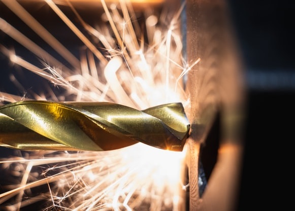
- Cutting Tools: hBN coatings improve tool life by reducing wear and providing self-lubricating properties, particularly in high-friction applications.
- Molds and Dies: The chemical inertness of hBN protects against corrosion and buildup, ensuring smooth operations in manufacturing processes.

Electronics
hBN thin films are ideal for electronic devices, where their dielectric properties and heat dissipation capabilities offer unparalleled advantages. Applications include:
- Insulating Layers: hBN coatings prevent electrical cross-talk in high-frequency devices, ensuring stability and performance.
- Encapsulation Layers: Their chemical inertness and thermal stability protect sensitive components in harsh environments, such as power electronics and 5G communication devices.
Optical Coatings
hBN’s transparency in the visible and infrared spectrum makes it a valuable material for optical coatings. Its applications include:
- Protective Layers for Lenses and Sensors: hBN coatings provide scratch resistance and chemical protection without compromising optical clarity.
- Infrared Windows: hBN thin films are used in sensors and cameras operating in extreme environments, enhancing durability while maintaining optical performance.
Case Studies and Practical Examples
- In a high-power LED system, hBN coatings enhance thermal management, ensuring stable performance and extending device lifespan.
- In industrial cutting tools, hBN thin films reduce wear rates by up to 40%, according to recent studies, providing significant cost savings in manufacturing.
The Role of hBN Sputtering Targets in PVD Processes
Hexagonal boron nitride (hBN) sputtering targets are at the heart of producing high-performance coatings via PVD techniques. These targets are carefully engineered to ensure consistent material deposition, meeting the stringent requirements of advanced applications. Their quality and design directly influence the properties of the resulting thin films.
Key Characteristics of hBN Sputtering Targets
- High Purity: High-purity hBN targets minimize contamination during the deposition process, ensuring thin films with exceptional dielectric and thermal properties.
- Density and Uniformity: Optimal target density reduces porosity and improves material ejection consistency during sputtering, leading to uniform coatings.
- Thermal Stability: hBN targets withstand high operating temperatures, making them reliable in demanding PVD environments.
Advantages in PVD Applications
hBN sputtering targets enable precise and efficient deposition of thin films for various industries. Benefits include:
- Versatile Film Customization: Targets allow control over film thickness, composition, and stoichiometry by adjusting PVD parameters.
- Scalability: From laboratory experiments to industrial production, hBN targets are suitable for both small-scale and large-scale coating needs.
- Reduced Defects: Advanced manufacturing processes for hBN targets reduce cracks and impurities, resulting in high-quality coatings.
Applications of hBN Sputtering Targets
- Electronics: Used to deposit insulating layers for semiconductor devices, hBN targets help achieve stable and high-performance coatings.
- Optical Coatings: hBN thin films, produced using sputtering targets, provide durable protective layers for lenses, sensors, and infrared windows.
- Industrial Tooling: High-purity hBN targets produce thin films that enhance the wear resistance and longevity of cutting tools and molds.
Factors Influencing Target Performance
- Target Composition: The quality and purity of the hBN material used in the target determine the thin film’s overall performance.
- Sputtering Power and Pressure: Optimized power levels and chamber pressure ensure consistent material ejection and film adhesion.
- Target Longevity: High-quality hBN targets exhibit longer lifespans, reducing operational costs in industrial settings.
6. Conclusion
Hexagonal boron nitride (hBN) thin films, deposited via PVD techniques, have revolutionized the field of high-performance coatings. Their exceptional thermal stability, electrical insulation, and chemical resistance make them indispensable in industries such as aerospace, electronics, and industrial tooling. By leveraging advanced PVD methods like magnetron sputtering and electron beam evaporation, manufacturers can achieve precise and customizable coatings tailored to the most demanding applications.
At the core of these processes are hBN sputtering targets, which ensure the uniformity, purity, and durability required for consistent results. These targets play a vital role in delivering thin films with superior performance, unlocking new possibilities in thermal management, corrosion resistance, and electrical insulation.
Whether for protecting critical aerospace components or enhancing the efficiency of semiconductor devices, hBN thin films exemplify the transformative potential of advanced materials in modern technology. For more information on hBN sputtering targets and their applications, visit Stanford Advanced Materials (SAM), your trusted partner in high-quality materials for PVD processes.
Reference:
[1] Graphene/(h-BN) n/X-doped graphene as anode material in lithium ion batteries (X=Li, Be, B and N). Macedonian Journal of Chemistry and Chemical Engineering. 36. 101. 10.20450/mjcce.2017.1134.
[2] Wu, Shilin & Shao, Tao & Zhang, Zhaotian & Huang, Lingyu. (2020). Effect of surface modification of electrodes on charge injection and dielectric characteristics of propylene carbonate. High Voltage. 5. 10.1049/hve.2019.0144.


