
Physical Vapor Deposition (PVD) is a widely used technique in various industries, such as electronics, optics, and materials science. It is crucial for depositing thin films onto substrates, which are essential in the manufacturing of components like semiconductors, mirrors, and solar panels. The quality, thickness, adhesion, and performance of the thin film depend largely on the PVD method chosen. Selecting the most suitable method for a given application ensures the desired properties of the film, making it vital to understand the different techniques available.
What is Physical Vapor Deposition (PVD)?
Physical Vapor Deposition (PVD) is a process where a material transitions from a solid phase to a vapor phase in a vacuum or low-pressure environment, and then the vaporized material condenses onto a substrate, forming a thin film. The process is typically carried out in a vacuum to avoid contamination and to maintain a clean deposition environment. PVD is widely used to deposit metals, alloys, ceramics, and other materials onto surfaces, improving their resistance to wear, corrosion, and other environmental factors.
Common PVD Methods
There are several PVD methods, each with unique characteristics and applications. The most commonly used methods are Sputtering, Thermal Evaporation, Ion Plating, and Laser Ablation (Pulsed Laser Deposition, PLD). If you want to see a full list of PVD Methods, you can read this article. Below, we will explore each of these 4 methods mentioned befor in detail to help you understand which one may be the best choice for your needs.
1. Sputtering Deposition
Sputtering is a versatile PVD method commonly used for depositing metals, ceramics, and composite thin films. During sputtering, high-energy ions bombard a target material (cathode), causing atoms to be ejected from the target. These ejected atoms then deposit onto a substrate, forming a thin film.
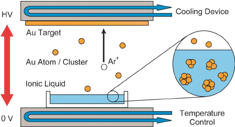
The process requires a power source (DC or RF) to generate the high-energy ions in the plasma.
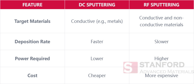
- DC Sputtering: This method is simple, cost-effective, and commonly used for conductive materials, such as metals. It is particularly suited for applications like semiconductor manufacturing and SEM sample preparation.
- RF Sputtering: RF sputtering alternates the polarity of the power supply, making it suitable for both conductive and non-conductive materials (e.g., ceramics, insulators). This method allows for a wider range of target materials compared to DC sputtering.
DC vs RF Sputtering Comparison:
2. Thermal Evaporation
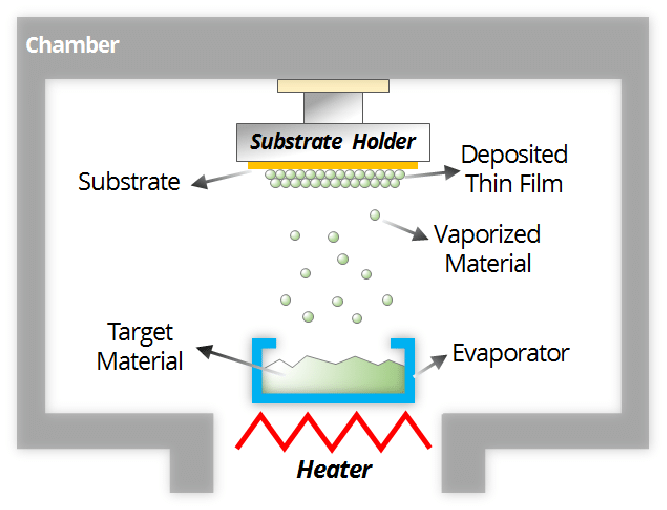
Thermal Evaporation is another popular PVD method, especially for depositing metals and organic materials. In this process, a material is heated to a high temperature in a vacuum until it evaporates. Once vaporized, the material condenses onto the cooler substrate, forming a thin film.
Thermal evaporation is often used for organic coatings and simpler metal films. It’s a relatively cost-effective method and is commonly used for applications where materials with lower melting points or simple coatings are required. However, it does have limitations when it comes to high-melting point materials or more complex films.
This method is also suitable for applications where lower deposition temperatures are required, or for processes with simpler material needs. However, the deposition rate tends to be lower than sputtering, and the film quality may vary depending on the material being deposited.
Advantages and Disadvantages of Thermal Evaporation:
- Advantages:
- Simpler process
- Cost-effective
- Low temperature deposition
- Disadvantages:
- Limited to materials with low to medium melting points
- Less control over film thickness and uniformity
- Not suitable for complex multilayer films
3. Ion Plating
Ion Plating (also known as Ion Vapor Deposition, or IVD) is a PVD method that combines vapor deposition with ion bombardment. In this process, the target material is first evaporated or sputtered in a vacuum, and then the vaporized material is ionized using a high-energy ion source. The ions are accelerated towards the substrate, where they bombard the deposited thin film.
Ion Plating has the advantage of significantly improving the adhesion and density of the thin films. The ion bombardment helps to pack the film more tightly, which results in a more durable and smooth coating. Additionally, the ion energy can help improve the coating’s properties, such as its hardness and resistance to wear.
Ion Plating is typically used for:
- Coating Hard Tools: Such as cutting tools and dies, where high hardness and wear resistance are crucial.
- Decorative Coatings: On jewelry, watches, and other products requiring both durability and aesthetic appeal.
- Optical Coatings: For enhanced performance in lenses and mirrors.
Advantages and Disadvantages of Ion Plating:
- Advantages:
- Enhanced film adhesion and density
- Improved film hardness and wear resistance
- Good for high-performance coatings
- Disadvantages:
- More complex process
- Requires more equipment and energy compared to simpler methods like thermal evaporation
- Deposition rate is lower than sputtering in some cases
4. Laser Ablation (Pulsed Laser Deposition, PLD)
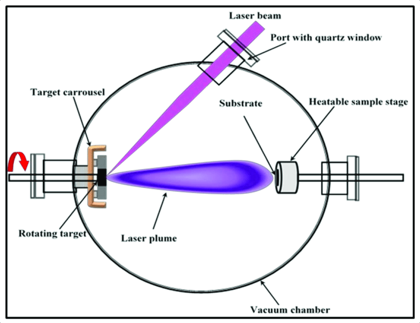
Laser Ablation, also known as Pulsed Laser Deposition (PLD), is a PVD method in which a high-powered laser pulse is directed onto a target material, causing it to ablate (vaporize) into a plasma. The vaporized material then deposits onto a substrate, forming a thin film. The process is performed in a vacuum or low-pressure environment to control the deposition.
PLD is widely used for depositing complex thin films, especially in the research and development of new materials, such as high-temperature superconductors, thin-film semiconductors, and advanced coatings. The laser provides high energy, which allows for the deposition of materials with high melting points and complex compositions.
The key advantages of PLD include its ability to deposit stoichiometric films, where the ratio of the components in the thin film is identical to the target material. This is important for applications where precise composition control is critical, such as in high-performance optical coatings and advanced semiconductor devices.
PLD is also highly versatile, allowing for the deposition of a wide variety of materials, including metals, insulators, and semiconductors. However, PLD requires precise control of laser parameters and is typically a slower process compared to other PVD techniques.
Advantages and Disadvantages of Laser Ablation (PLD):
- Advantages:
- High precision in material composition
- Suitable for complex materials and high-melting-point substances
- Versatile, capable of depositing a wide range of materials
- Ideal for research and development applications
- Disadvantages:
- Slower deposition rate compared to sputtering and thermal evaporation
- Expensive equipment and high operational costs
- Requires precise control of laser parameters
How to Choose the Right PVD Method?
When choosing between sputtering, thermal evaporation, ion plating, and laser ablation, several factors need to be considered, including:
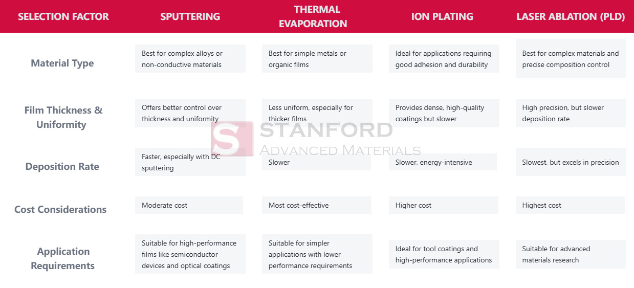
- Material Type: If you’re working with non-conductive materials or complex alloys, sputtering (especially RF sputtering) is often the better choice. For simple metals or organic films, thermal evaporation may be more suitable. If adhesion and durability are critical, ion plating may be ideal. For highly complex materials or precise composition control, PLD is recommended.
- Film Thickness and Uniformity: Sputtering generally offers better control over film thickness and uniformity, especially for films that need to be precisely controlled. Thermal evaporation may result in less uniform coatings, particularly for thicker films. Ion plating provides dense, high-quality coatings, but the process may be slower and more energy-intensive. PLD, while precise, typically has a slower deposition rate.
- Deposition Rate: If deposition speed is critical, DC sputtering tends to have a higher deposition rate compared to thermal evaporation. Ion plating usually has a lower deposition rate than both sputtering and thermal evaporation, but provides superior coating properties. PLD is generally the slowest method but excels in precision and material control.
- Cost Considerations: Thermal evaporation tends to be the most cost-effective method compared to sputtering, ion plating, and PLD. However, PLD and ion plating offer superior film quality and performance, which may justify their higher costs for advanced applications.
- Application Requirements: For thin films requiring high performance, such as those used in semiconductor devices or optical coatings, sputtering is generally preferred. Ion plating is ideal for tool coatings and high-performance applications. PLD is suited for advanced materials research, while thermal evaporation is best for simpler applications with lower performance demands.
Summary
In conclusion, Sputtering, Thermal Evaporation, Ion Plating, and Laser Ablation (PLD) are four widely used PVD methods, each with its unique strengths. Sputtering is suitable for high-precision applications requiring complex materials and thin, uniform films. Thermal evaporation is cost-effective for simpler coatings and organic films, while ion plating offers enhanced adhesion, hardness, and wear resistance for tool coatings and high-performance applications. PLD excels in depositing complex materials with precise composition control, making it ideal for research and advanced semiconductor devices. By considering factors such as material type, film quality requirements, deposition rate, and cost, you can choose the most suitable PVD method to achieve the desired properties for your application.
Stanford Advanced Materials (SAM) is a trusted global supplier of high-quality evaporation material and sputtering targets. We offer a comprehensive range of metals, alloys, oxides, and ceramic materials to meet your industrial needs at competitive prices. Stay informed about the latest advancements in PVD and related technologies by visiting our website.
Reference
Hatakeyama, Yoshikiyo & Onishi, Kei & Nishikawa, Keiko. (2011). Effects of sputtering conditions on formation of gold nanoparticles in sputter deposition technique. RSC Adv.. 1. 1815-1821. 10.1039/C1RA00688F.
Park, Sung-Ik & Quan, Yingjun & Kim, Se-Heon & Kim, Hyungsub & Kim, Sooyeun & Chun, Doo-Man & Lee, Caroline & Taya, Minoru & Chu, Won-Shik & Ahn, Sung-Hoon. (2016). A review on fabrication processes for electrochromic devices. International Journal of Precision Engineering and Manufacturing-Green Technology. 3. 397-421. 10.1007/s40684-016-0049-8.
Ogugua, Simon & Swart, H. & Ntwaeaborwa, Odireleng. (2020). Latest Development on Pulsed Laser Deposited ThinFilms for Advanced Luminescence Applications. Coatings. 10. 1078. 10.3390/coatings10111078.


