Effect of Sputtering Target Purity on Large-Area Coating Production
The requirement of the target quality for sputter coating is higher than that of the traditional materials industry.
When the substrate enters the high vacuum coating chamber, if the sputtering target is not pure enough, under the action of the electric field and the magnetic field, the impurity particles in the target will adhere to the substrate surface during the sputtering process. This will affect the film’s firmness, and even the film layer will fall off. Therefore, the higher the purity of the target, the better the performance of the coating film.

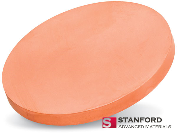
Take Copper (Cu) Sputtering Target for an example. In the preparation of copper sputtering target, it is inevitable to introduce other impurity contents such as sulfur and lead elements. A trace amount of sulfur can prevent the grain size from increasing or causing microcracks during hot working; however, when the sulfur element content is higher than 18 ppm, microcracks appeared; as the content of two impurity elements (sulfur and lead) increases, the number of target cracks and the number of arcing discharges will increase. Therefore, the impurity content in the target should be reduced as much as possible to improve the uniformity of the film.

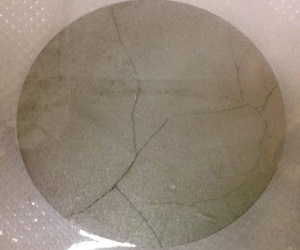
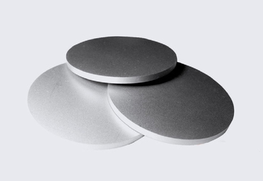
For targets with poor thermal conductivity, such as SiAl targets, the heat transfer is hindered due to the target impurity, which causes cracking of the target during use. Under normal circumstances, slight cracks will not have a great impact on the coating production, but when the target has obvious cracks, the charge is very easy to concentrate at the edge of the crack, resulting in the abnormal discharge of the target. The discharge phenomenon will lead to the occurrence of slag, abnormal film formation, and increased product scrap. Therefore, in the process of preparing the target, the purity of the targets should be controlled.
Stanford Advanced Materials (SAM) Corporation is a global sputtering targets manufacturer established in 1994. We specialize in producing high puritysputtering target with the highest possible density and smallest possible average grain sizes for use in semiconductor, chemical vapor deposition (CVD) and physical vapor deposition (PVD) display and optical applications. Please visit our website https://www.sputtertargets.net/ for more information.


