Introduction
Background of Sputtering Technology
Thin film deposition is a cornerstone in the fabrication of modern technological devices. From electronic components to optical coatings, the demand for high-quality thin films has surged, driving advancements in deposition techniques. Among these, sputtering has emerged as a versatile and reliable method, offering precise control over film composition and thickness.
Sputtering involves the ejection of atoms from a solid target material due to bombardment by energetic ions, typically generated in a plasma environment. This process occurs under vacuum conditions, where the sputtered atoms condense onto a substrate, forming a thin film. The efficiency and quality of the deposited film depend on various factors, including the type of sputtering technique employed.
This article aims to provide an in-depth comparison between DC Sputtering and Magnetron Sputtering. By exploring their operational mechanisms, equipment configurations, process parameters, and respective advantages and limitations, readers will gain a clearer understanding of which method best suits their specific application requirements.
Overview of Sputtering Technology
Sputtering is a physical vapor deposition (PVD) technique used to deposit thin films by ejecting material from a target source onto a substrate. The process utilizes a plasma to generate ions that bombard the target material, causing atoms to be dislodged and subsequently deposited as a film.
Sputtering can be classified based on various criteria:
- Power Source:
- Direct Current (DC) Sputtering: Utilizes a constant DC power supply.
- Radio Frequency (RF) Sputtering: Employs an alternating power source, suitable for insulating targets.
- Magnetic Field Application:
- Non-Magnetron Sputtering: Relies solely on the electric field for plasma generation.
- Magnetron Sputtering: Incorporates magnetic fields to enhance plasma density and sputtering efficiency.
Sputtering is versatile and finds applications in:
- Electronics: Deposition of conductive and semiconductive layers in integrated circuits and displays.
- Optical Coatings: Creation of high-reflectivity mirrors, anti-reflective coatings, and laser optics.
- Semiconductor Manufacturing: Formation of barrier layers, dielectric films, and conductive interconnects.
- Decorative and Functional Coatings: Enhancing surface properties such as hardness, wear resistance, and aesthetic appeal.
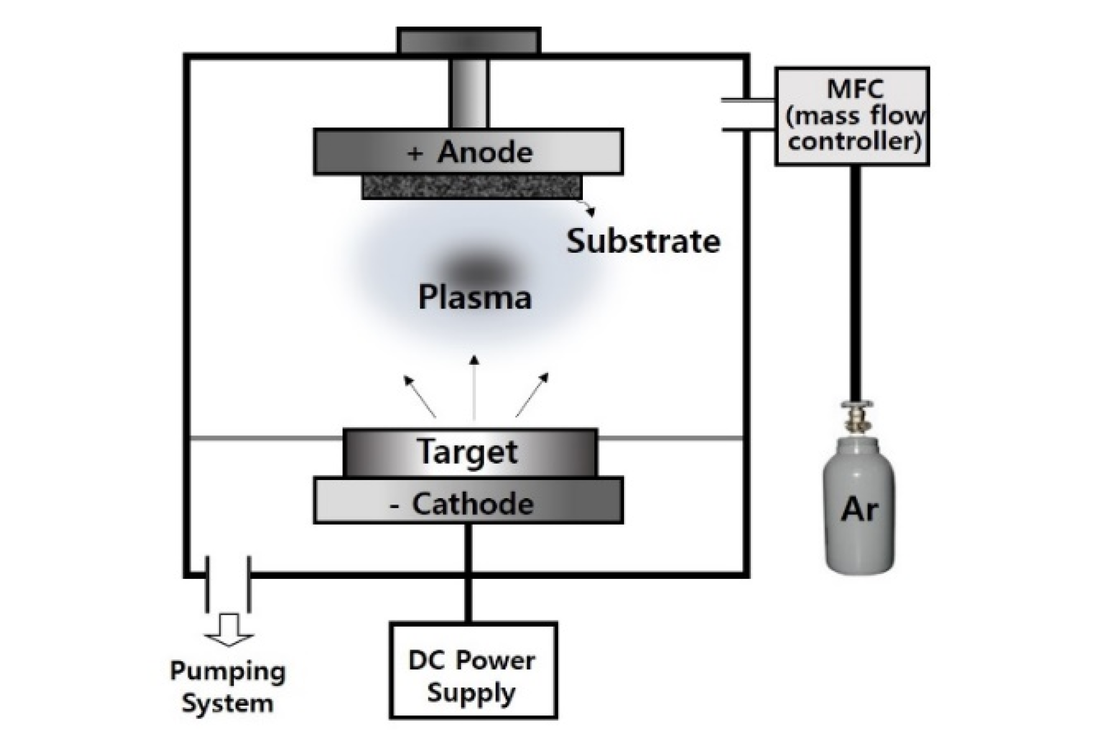
Direct Current (DC) Sputtering
DC Sputtering operates by applying a constant direct current between the cathode (target) and the anode within a vacuum chamber. This generates a plasma consisting of ions, typically Argon (Ar), which bombard the target material. The energy from these ions dislodges atoms from the target, which then migrate and deposit onto the substrate, forming a thin film.
Kim, Hyun-Ji & Kang, Gi-Hwan & Kim, Sung-Hoon & Park, Sangmoon. (2020). Enhancement of Electromagnetic Wave Shielding Effectiveness of Carbon Fibers via Chemical Composition Transformation Using H2 Plasma Treatment. Nanomaterials. 10. 1611. 10.3390/nano10081611.
Equipment and Process Parameters
- Vacuum Level: Typically maintained between 10−3 to 10−6 Torr to ensure a stable plasma and minimize contamination.
- Working Gas: Argon is commonly used due to its inert nature and optimal ionization properties.
- Voltage and Current: The DC power supply provides a steady voltage and current, with voltage levels and current densities adjusted based on target material and desired deposition rates.
Advantages
- Simplicity: The operation and equipment setup for DC sputtering are straightforward, making it accessible for various applications.
- Cost-Effectiveness: Lower initial and maintenance costs compared to more complex sputtering systems.
- Suitability for Medium to Small-Scale Production: Ideal for applications where high-volume production is not critical.
Disadvantages
- Material Limitations: Only conductive target materials can be sputtered effectively, restricting the range of applicable materials.
- Low Target Utilization Efficiency: Typically, only 10%-20% of the target material is utilized before significant erosion occurs.
- Uniformity Challenges: Achieving uniform thin film deposition, especially over large substrates, can be difficult.
Typical Applications
- Metal Thin Films: Deposition of metals such as aluminum, titanium, and copper for electronic components.
- Simple Electronic Components: Ideal for manufacturing basic electronic devices where high precision is not paramount.
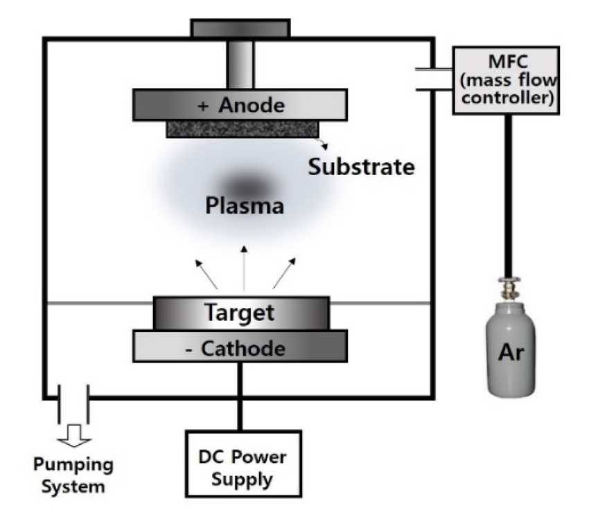
Magnetron Sputtering
Magnetron Sputtering enhances the basic sputtering process by introducing a magnetic field near the target surface. This magnetic field confines electrons, increasing the plasma density and ionization efficiency. Consequently, more ions bombard the target, improving the sputtering rate and overall deposition efficiency.

Equipment and Process Parameters
- Magnetic Field Configuration: Strategic placement and strength of magnets are crucial to confine electrons and sustain high plasma densities.
- Gas Pressure: Typically lower than in DC sputtering, around 0.1-1 Torr, to optimize plasma stability and sputtering efficiency.
- Power Density: Higher power densities are employed to maintain the enhanced plasma conditions necessary for efficient sputtering.
Advantages
- Higher Target Utilization Efficiency: Utilizes between 20%-30% of the target material, reducing waste and cost.
- Increased Deposition Rates: Enhanced plasma density leads to faster film deposition, boosting production throughput.
- Improved Thin Film Quality: Better uniformity and adhesion result in higher-quality films, essential for advanced applications.
- Lower Operating Temperatures: Suitable for heat-sensitive substrates, broadening the range of materials that can be effectively coated.
Disadvantages
- Complexity: More intricate equipment design and setup compared to DC sputtering.
- Higher Initial Investment: Greater upfront costs due to additional components like magnets and more sophisticated power supplies.
- Maintenance and Operation: Requires specialized knowledge for optimal magnetic field configuration and system maintenance.
Typical Applications
- Semiconductor Device Manufacturing: Deposition of metal interconnect layers and barrier films in integrated circuits.
- Optical Coatings: Production of anti-reflective coatings and multilayer optical filters with precise thickness control.
- Decorative Coatings: High-quality, wear-resistant coatings for automotive parts and electronic devices, enhancing both aesthetics and functionality.
Comparison between DC Sputtering and Magnetron Sputtering
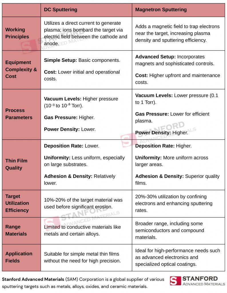
Comparison of Working Principles
- DC Sputtering: Relies solely on a direct current source to generate plasma, with ion bombardment driven by the electric field between the cathode and anode.
- Magnetron Sputtering: Incorporates a magnetic field to trap electrons near the target, significantly increasing plasma density and ionization rates, thereby enhancing sputtering efficiency.
Equipment Complexity and Cost
- DC Sputtering:
- Complexity: Simple setup with basic components.
- Cost: Lower initial and operational costs, making it accessible for a wide range of applications.
- Magnetron Sputtering:
- Complexity: Advanced setup incorporating magnets and more sophisticated control systems.
- Cost: Higher upfront and maintenance costs due to the additional magnetic and electrical components.
Process Parameters
- Vacuum Levels: DC sputtering operates at higher pressures (10−3 to 10−6 Torr) compared to magnetron sputtering (0.1 to 1 Torr).
- Gas Pressures: Lower gas pressures in magnetron sputtering contribute to more efficient plasma generation.
- Power Densities: Magnetron sputtering utilizes higher power densities to sustain the enhanced plasma conditions.
Thin Film Quality
- Deposition Rate: Magnetron sputtering generally achieves higher deposition rates due to increased plasma density.
- Film Uniformity: Superior in magnetron sputtering, ensuring consistent film thickness across larger substrates.
- Adhesion and Density: Films produced via magnetron sputtering exhibit better adhesion to substrates and higher density, enhancing their mechanical and electrical properties.
Target Utilization Efficiency
- DC Sputtering: Utilizes only 10%-20% of the target material before significant erosion.
- Magnetron Sputtering: Improves target utilization to 20%-30% by confining electrons and enhancing sputtering rates.
Range of Applicable Materials
- DC Sputtering: Limited to conductive materials, restricting its use to metals and certain alloys.
- Magnetron Sputtering: Capable of sputtering a broader range of materials, including some semiconductors and compound materials, expanding its applicability.
Differences in Application Fields
- DC Sputtering: Suited for simple metal thin film applications where high precision and complex structures are not required.
- Magnetron Sputtering: Ideal for high-performance applications demanding high-quality, uniform, and adherent films, such as in advanced electronics and specialized optical coatings.
Latest Developments and Cutting-Edge Technologies
High Power Impulse Magnetron Sputtering (HiPIMS)
HiPIMS is an advanced form of magnetron sputtering that employs high-power pulses with low duty cycles. This results in a highly ionized plasma, leading to superior film quality and enhanced film properties.
- Features and Advantages:
- Higher Ionization Rates: Facilitates better control over film composition and microstructure.
- Superior Film Quality: Produces denser and more uniform films with improved mechanical and electrical properties.
- Application Examples:
- High-Precision Electronic Devices: Ensures reliable performance in sensitive electronic components.
- Advanced Optical Coatings: Achieves optimal optical properties for high-performance lenses and mirrors.
Reactive Sputtering Technologies
Reactive sputtering involves introducing reactive gases (e.g., oxygen, nitrogen) into the sputtering chamber to form compound thin films such as oxides, nitrides, and carbides.
- Applications:
- Oxide Thin Films: Production of materials like TiO₂ and SiO₂ for optical and electronic applications.
- Nitride Thin Films: Synthesis of films such as TiN for hard coatings and diffusion barriers.
- Enhancements:
- Film Functionality: Reactive sputtering allows for the creation of films with tailored chemical and physical properties.
- Diversity: Enables the deposition of a wide range of compound materials, expanding application possibilities.
Sputtering for Nanostructured Thin Films
Nanostructured thin films exhibit unique properties due to their nanoscale features, making them valuable in advanced technological applications.
- Methods and Techniques:
- Pulsed Sputtering: Utilizes controlled pulses to create nanostructures.
- Substrate Biasing: Enhances film adhesion and density, promoting nanostructure formation.
- Characteristics and Applications:
- Nanoelectronics: Enables the fabrication of components with enhanced electrical properties.
- Enhanced Coatings: Provides improved surface hardness, wear resistance, and functional properties for various industrial applications.
Case Studies of Practical Applications
Sputtering in the Semiconductor Industry
Sputtering technologies are integral to the semiconductor manufacturing process, where precision and reliability are paramount.
- Deposition Processes and Performance Requirements:
- Metal Interconnects: Magnetron sputtering is preferred for depositing copper and aluminum interconnects due to its high deposition rates and excellent film uniformity.
- Barrier Layers: Sputtering of materials like TiN ensures effective diffusion barriers, essential for preventing metal migration.
- Application of DC and Magnetron Sputtering:
- DC Sputtering: Used in early-stage deposition processes where simplicity and cost-effectiveness are beneficial.
- Magnetron Sputtering: Employed in advanced stages requiring high-quality, dense, and uniform films.
Sputtering in Optical Coatings
Optical coatings require precise control over film thickness and composition to achieve desired optical properties.
- Manufacturing of Multilayer Structures and Anti-Reflective Coatings:
- Multilayer Structures: Magnetron sputtering facilitates the sequential deposition of multiple layers with exact thickness control, essential for achieving specific reflective and refractive properties.
- Anti-Reflective Coatings: High uniformity and precise composition achieved through magnetron sputtering enhance the performance of lenses and display screens.
- Advantages of Magnetron Sputtering:
- High-Quality Optical Films: Ensures minimal defects and optimal optical performance.
- Scalability: Suitable for large-scale production of high-performance optical components.
Decorative and Functional Coatings
Sputtering is utilized to enhance both the aesthetic and functional properties of various products.
- Color Control and Surface Hardening:
- Color Control: Magnetron sputtering allows for precise control over film composition, enabling a wide range of colors and finishes.
- Surface Hardening: Sputtered coatings improve surface hardness, providing resistance to wear and corrosion.
- Application of DC and Magnetron Sputtering:
- DC Sputtering: Suitable for simple decorative layers where high precision is not critical.
- Magnetron Sputtering: Ideal for producing high-wear-resistant and durable coatings required in automotive parts and consumer electronics.
Conclusion
DC sputtering is ideal for producing simple and cost-effective metal thin films. Its straightforward setup and lower operational costs make it suitable for medium to small-scale manufacturing where high production volumes and complex film properties are not necessary. Conversely, magnetron sputtering excels in applications that require high-quality and uniform thin films. This technique is essential for advanced electronics, optical coatings, and various functional surface treatments due to its ability to create dense and adherent coatings. Choosing between DC sputtering and magnetron sputtering depends on the specific needs of the application, including factors like film complexity, production scale, and desired material properties.
Stanford Advanced Materials provides high-quality targets suitable for various sputtering methods, meeting diverse technical needs and helping customers achieve optimal thin film performance.


