
Thin film coating materials play a crucial role in modern industries and technological fields, with widespread applications in electronics, optics, energy, biomedicine, and more. Understanding the classification of thin film materials, specific materials, deposition methods, and their applications helps in making optimal choices and optimizing processes in practical applications. This guide delves into the various classifications of thin film coating materials and their specific applications.
I Classification by Deposition Method
There are numerous methods for preparing thin film materials, each with unique advantages and suitable materials. The primary deposition methods include Physical Vapor Deposition (PVD), Chemical Vapor Deposition (CVD), Solution-Based Methods, and Electroplating.
1. Physical Vapor Deposition (PVD)
Physical Vapor Deposition is a technique that transfers material from the vapor phase to the substrate surface through physical processes. Common PVD methods include sputtering, evaporation, and Pulsed Laser Deposition (PLD).
Sputtering
- Materials: Aluminum (Al), Titanium (Ti), Nickel (Ni), Copper (Cu), Titanium Nitride (TiN), Chromium Oxide (Cr₂O₃).
- Applications: Suitable for manufacturing electronic circuits, optical coatings, and forming protective layers. Due to its good adhesion and high purity, it is commonly used in fields requiring high-quality thin films.
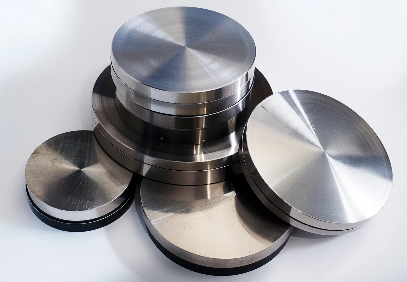
- Sputtering Targets: The choice of Sputtering Targets is crucial as they serve as the source material in the sputtering process. High-purity and appropriately selected targets ensure efficient deposition and superior film quality.
Evaporation
- Materials: Pure Gold (Au), Silver (Ag), Tungsten (W), Organic Materials.
- Applications: Often used for producing mirrors, optical coatings, and decorative thin films. Its high purity and relatively low deposition temperatures make it suitable for coating temperature-sensitive substrates.
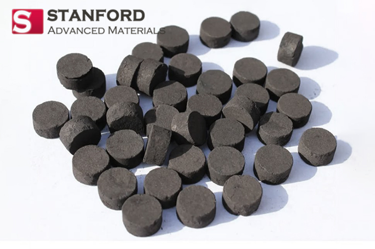
- Evaporation Materials: Selecting the right Evaporation Materials is essential for achieving the desired film properties. These materials must have suitable vapor pressures and thermal stability to ensure consistent and uniform deposition.
Pulsed Laser Deposition (PLD)
- Materials: Complex Oxides, Multi-Component Materials.
- Applications: Ideal for fabricating high-quality single-crystal thin films and thin-film electronic devices, especially those requiring high uniformity and complex compositions.
Magnetron Sputtering
- Materials: High-Melting-Point Metals (e.g., Tungsten), Insulating Materials (e.g., Al₂O₃).
- Applications: Suitable for large-area coatings and electronic packaging, achieving high coverage and uniformity. Widely used in the manufacture of flat-panel displays and solar cells.
2. Chemical Vapor Deposition (CVD)
Chemical Vapor Deposition is a method that converts gaseous precursors into solid thin films through chemical reactions. Major CVD types include Thermal CVD, Plasma-Enhanced CVD (PECVD), and Atomic Layer Deposition (ALD).
-
Thermal CVD
- Materials: Silicon-based Materials (e.g., Si), Metal Oxides (e.g., TiO₂).
- Applications: Suitable for manufacturing semiconductor devices and large-scale production, capable of forming high-quality silicon thin films and metal oxide coatings. Widely used in integrated circuits and solar cells.
-
Plasma-Enhanced CVD (PECVD)
- Materials: Silicon Dioxide (SiO₂), Silicon Nitride (Si₃N₄).
- Applications: Used for depositing electronic insulating layers and optical coatings, offering the advantage of low-temperature deposition. Suitable for temperature-sensitive substrates like flexible electronics.
-
Atomic Layer Deposition (ALD)
- Materials: High-K Dielectric Materials (e.g., HfO₂), Aluminum Oxide (Al₂O₃).
- Applications: Ideal for nanoscale processes and advanced semiconductor device manufacturing, enabling exceptionally uniform thin films with precise thickness control. Essential for high-performance electronic devices.
3. Solution-Based Methods
Solution-based methods form thin films through chemical precursors in a solution at the substrate surface. Common techniques include sol-gel, spray coating, and spin coating.
-
Sol-Gel Method
- Materials: Metal Oxides (e.g., SiO₂, TiO₂), Ceramic Materials.
- Applications: Suitable for large-area coatings and optical coatings, commonly used in solar cells, optical lenses, and protective coatings.
-
Spray Coating
- Materials: High-Viscosity Precursors.
- Applications: Used for rapid coating and thick film fabrication, suitable for large-scale industrial applications such as automotive coatings and construction materials.
-
Spin Coating
- Materials: Photoresists, Polymers (e.g., PMMA, PI).
- Applications: Widely used in electronic displays, polymer thin film fabrication, and micro/nano-electronic device manufacturing due to its high uniformity and controllability.
4. Electroplating
Electroplating involves depositing metals onto a substrate through electrochemical reactions and is a common deposition method applicable to various metals.
- Materials: Nickel (Ni), Copper (Cu), Gold (Au), Silver (Ag).
- Applications: Extensively used in manufacturing electronic components, surface treatment of automotive parts, and producing decorative coatings. Its high coverage and excellent electrical conductivity make it indispensable in high-performance electronic devices and precision industries.
II. Classification by Material Type
Based on inherent properties, thin film materials can be categorized into metal thin films, insulating thin films, semiconductor thin films, polymer thin films, and ceramic/glass thin films.
1. Metal Thin Films
Metal thin films are widely used across multiple fields due to their excellent electrical conductivity and corrosion resistance.
-
- Materials: Aluminum (Al), Gold (Au), Silver (Ag), Titanium (Ti).
- Properties: High electrical conductivity, good corrosion resistance, and high reflectivity.
- Applications: Primarily used in electronic circuits, mirror fabrication, and decorative coatings. For example, aluminum thin films are commonly used in semiconductor interconnects, and gold thin films are used in high-reliability electronic contact points.
-
- Materials: Titanium Nitride (TiN), Chromium Oxide (Cr₂O₃).
- Properties: Higher hardness and corrosion resistance compared to pure metal thin films, with superior mechanical properties.
- Applications: Widely used in aerospace, automotive industries, and protective coatings. TiN is commonly used for hardening tool surfaces, and Cr₂O₃ is used for protective coatings in chemical equipment.
2. Insulating Thin Films
Insulating thin films are primarily used for insulating electronic devices and optical coatings, offering high insulation performance and chemical stability.
-
- Materials: Silicon Dioxide (SiO₂), Aluminum Oxide (Al₂O₃), Titanium Dioxide (TiO₂), Zinc Oxide (ZnO).
- Properties: Excellent insulation properties, chemical stability, and transparency.
- Applications: Used as insulating layers in electronic devices, optical coatings, and gas sensors. For example, SiO₂ is commonly used in MOS capacitors and gate dielectrics, while Al₂O₃ is used in high-K capacitors.
-
- Materials: Silicon Nitride (Si₃N₄), Aluminum Nitride (AlN).
- Properties: High hardness, excellent thermal stability, and mechanical strength.
- Applications: Widely used in electronic packaging, protective coatings, and optical applications. Si₃N₄ is used as a protective layer in integrated circuits, and AlN is used for thermal management and high-frequency circuits substrates.
3. Semiconductor Thin Films
Semiconductor thin films play a critical role in electronic and optoelectronic devices, offering high electron mobility and excellent light absorption capabilities.
-
- Materials: Polycrystalline Silicon, Amorphous Silicon.
- Applications: Primarily used in solar cells and thin-film transistors, with amorphous silicon widely used in thin-film solar cells and liquid crystal displays.
-
Other Semiconductor Materials
- Materials: Gallium Nitride (GaN), Cadmium Telluride (CdTe).
- Properties: High electron mobility and high light absorption efficiency, suitable for high-performance electronic devices and efficient light-to-electricity conversion.
- Applications: GaN is used in LEDs and high-frequency, high-power electronic devices, while CdTe is used in high-efficiency solar cells and photodetectors.
4. Polymer Thin Films
Polymer thin films are widely used in displays, optical lenses, and flexible electronic devices due to their mechanical flexibility and high transparency.
-
Pure Polymer Thin Films
- Materials: Polystyrene (PS), Poly(methyl methacrylate) (PMMA), Polyimide (PI).
- Properties: Good mechanical flexibility, high transparency, and ease of processing.
- Applications: Used as substrates for display screens, optical lenses, and flexible electronic device substrates. PMMA, for example, is commonly used in optical lenses and protective layers for LCD displays.
-
Functional Polymer Thin Films
- Materials: Conductive Polymers (e.g., PEDOT:PSS), Photosensitive Polymers.
- Applications: Widely used in sensors, optoelectronic devices, and flexible electronics. PEDOT:PSS is used as electrode layers in organic light-emitting diodes (OLEDs) and touch screens.
5. Ceramic and Glass Thin Films
Ceramic and glass thin films are valued for their high hardness, wear resistance, and chemical stability, making them suitable for protective coatings, high-temperature environments, and optical devices.
-
Ceramic Thin Films
- Materials: Aluminum Oxide (Al₂O₃), Titanium Dioxide (TiO₂), Zirconium Oxide (ZrO₂).
- Properties: High hardness, wear resistance, and excellent chemical stability, maintaining performance at high temperatures.
- Applications: Used for protective coatings, materials protection in high-temperature environments, and optical device coatings. For instance, Al₂O₃ is used for wear-resistant tool coatings, and ZrO₂ is used for protective layers in advanced ceramic devices.
-
Glass Thin Films
- Materials: Silicate Glass, Optical Glass.
- Applications: Primarily used for protection in optical devices and as cover layers for displays, providing transparency and weather resistance.
III. Classification by Function or Application
Based on their practical uses, thin film materials can be categorized into optical films, protective films, electronic and semiconductor application films, energy-related films, and biomedical films.
1. Optical Films
Optical films control the reflection, transmission, and absorption of light to enhance the performance and efficiency of optical devices.
-
Mirror Coatings
- Materials: Aluminum (Al), Silver (Ag), Gold (Au).
- Applications: Used in optical instruments, laser devices, and reflective mirrors, providing high reflectivity and excellent optical performance. For example, high-purity aluminum coatings are used in laser mirrors.
-
- Materials: Silicon Dioxide (SiO₂), Silicon Nitride (Si₃N₄).
- Applications: Applied to optical lenses, displays, and optical communication devices to reduce reflection losses and increase light transmission. For example, SiO₂ anti-reflective coatings are used on display screens to minimize glare.

-
Filter Films
- Materials: Specific spectral control materials, such as coated oxides and sulfides.
- Applications: Used in photographic filters, microscopes, and optical communication devices to selectively transmit specific wavelengths of light, enhancing image quality and signal transmission efficiency.
2. Protective Films
Protective films provide surface hardness and chemical corrosion resistance, extending the lifespan of devices.
-
Wear-Resistant Coatings
- Materials: Titanium Nitride (TiN), Aluminum Oxide (Al₂O₃).
- Applications: Used on tools, mechanical parts, and electronic contact points, offering high hardness and wear resistance. For example, TiN coatings on cutting tools significantly enhance their durability.
-
Corrosion-Resistant Coatings
- Materials: Chromium Oxide (Cr₂O₃), Titanium Nitride (TiN).
- Applications: Applied to chemical equipment, marine facilities, and automotive components to resist acid, alkali, and salt spray corrosion. For instance, Cr₂O₃ coatings on reactor interiors prevent corrosion.
3. Electronic and Semiconductor Application Films
Electronic and semiconductor thin films are fundamental to modern electronic devices, determining their performance and functionality.
-
Conductive Layers
- Materials: Gold (Au), Silver (Ag), Copper (Cu), Conductive Polymers (e.g., PEDOT:PSS).
- Applications: Used in electrodes, interconnects, and contact points. For example, metal interconnect layers in integrated circuits and conductive polymer electrodes in OLED displays.
-
Insulating Layers
- Materials: Silicon Dioxide (SiO₂), Silicon Nitride (Si₃N₄), Aluminum Oxide (Al₂O₃).
- Applications: Used as insulating layers in multilayer circuit boards and semiconductor devices. Examples include SiO₂ gate dielectrics in MOSFETs and Al₂O₃ insulating layers in multilayer ceramic capacitors.
-
Semiconductor Layers
- Materials: Silicon (Si), Gallium Nitride (GaN), Cadmium Telluride (CdTe).
- Applications: Used in transistors, photodiodes, and solar cells. Examples include GaN-based LEDs and Si-based thin-film transistors in display technologies.
4. Energy-Related Films
Energy-related thin films enhance photoelectric conversion efficiency and ionic conductivity, advancing renewable and clean energy technologies.
-
Solar Cell Materials
- Materials: Cadmium Telluride (CdTe), Copper Indium Gallium Selenide (CIGS), Polycrystalline Silicon.
- Applications: Used in photovoltaic panels and wearable energy devices to improve the light-to-electricity conversion efficiency. For example, CdTe thin-film solar cells are widely used in ground-based photovoltaic systems.
-
Electrolyte Films for Batteries
- Materials: Lithium Phosphorus Oxynitride (LiPON), Solid Electrolytes.
- Applications: Used in solid-state batteries and energy storage devices to enhance ionic conductivity and battery stability.
5. Biomedical Films
Biomedical thin films are essential in medical devices and applications, providing biocompatibility and functional surfaces.
-
Biocompatible Coatings
- Materials: Titanium Dioxide (TiO₂), Hydroxyapatite (HA).
- Applications: Used on medical implants and devices to promote biocompatibility and prevent rejection. For example, HA coatings on orthopedic implants encourage bone integration.
-
Antimicrobial Films
- Materials: Silver Nanoparticles, Copper Oxide (CuO).
- Applications: Applied to medical devices and surfaces to prevent bacterial growth and reduce infection risks.
IV. Deposition Method Selection Guidelines
Choosing the appropriate deposition method depends on various factors, including material properties, substrate type, desired film thickness, and application requirements.
- Material Compatibility: Ensure the deposition method is compatible with the chosen material’s physical and chemical properties.
- Substrate Sensitivity: Sensitive substrates may require low-temperature deposition methods like PECVD or ALD.
- Film Uniformity and Thickness Control: Methods like ALD offer precise thickness control and uniformity, suitable for nanoscale applications.
- Production Scale and Cost: Large-scale industrial production may favor methods like sputtering or electroplating for their scalability and cost-effectiveness.
- Application-Specific Requirements: Certain applications may demand specific film properties, such as high hardness for protective coatings or high conductivity for electronic interconnects.
Ⅴ. Conclusion
Thin film coatings are vital in industries such as electronics, optics, energy, and biomedicine. Selecting the appropriate deposition methods and material types is essential for enhancing performance and efficiency. As technological advancements drive the need for more diverse and high-quality thin films, Stanford Advanced Materials provides a wide range of coating materials to meet these evolving demands. By offering versatile and reliable solutions, Stanford Advanced Materials (SAM) supports innovation and excellence across various applications, enabling researchers and engineers to advance their projects effectively.


