Since ancient times, gold has been revered as a highly valuable material. From making jewelry to cookware and industrial materials, gold has proven to be very useful and precious to man, particularly because of its high malleability, ductility, and lustrous nature. Gold is one of the most precious metals known to man, and it has various applications. Other properties of gold that make it very useful are its electrical and thermal conductivity.
Gold thin films can be deposited on other materials, where they are used as layers or coatings in the production of sensors, semiconductors, batteries, and data storage. This article will explain the meaning of gold sputtering targets, their properties, and their applications.
What is Gold Sputtering Target?
In general, sputtering is a process in which microscopic particles of solid materials are ejected from the element’s surface. The ejected materials are used to coat another surface known as the substrate. The main essence of sputtering is to produce a source of deposition material for the substrate. Sputtering is mostly used in the electronics industry and is available with several metals, including gold. Gold sputtering requires a specialized sputtering device and carefully controlled conditions. In this process, discs of gold, known as sputtering targets, are placed within a vacuum chamber. High-energy ions bombard these targets, causing the gold atoms to sputter into the vapor phase. The vaporized gold then travels and condenses onto the substrate, forming a thin coating.
Like other sputtering target materials, gold targets have similar properties as pure metal gold but also possess specific characteristics tailored for sputtering applications.
Basic Element Properties:
- Atomic Number: 79
- Relative Atomic Mass: 196.966569(4) Dalton (The number in parentheses indicates the uncertainty in the measurement)
- Natural Occurrence: Gold is a dense, naturally occurring heavy metal, typically found in rocks and occasionally as flakes.
Physical Properties:
- Density: Approximately 19.32 g/cm³, contributing to a high sputtering rate.
- Melting Point: 1064°C, ensuring stability under high-energy conditions during sputtering.
- Mechanical Strength: Pure gold is relatively soft. To enhance mechanical stability during sputtering, gold targets are often alloyed with other metals or engineered with specific designs to prevent deformation and breakage.
- Thermal Conductivity: High thermal conductivity helps in dissipating heat generated during the sputtering process, maintaining target integrity.
Chemical Properties:
- Purity: High-purity gold targets (typically 99.99% or higher) are essential to minimize impurities that could adversely affect the quality of the deposited film.
- Chemical Stability: Gold is chemically inert and resistant to oxidation, ensuring consistent performance and longevity of the sputtering target under vacuum conditions.
Sputtering-Specific Characteristics:
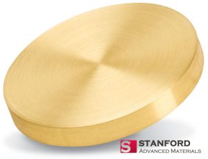
- Target Shape and Size: Gold sputtering targets are usually fabricated as circular discs with precise diameter and thickness specifications tailored to the sputtering equipment and specific process requirements. Uniform shape ensures consistent erosion rates and film deposition.
- Surface Roughness: The surface of the sputtering target is meticulously polished to achieve minimal roughness, which is critical for producing uniform thin films without defects.
- Electrical Conductivity: Excellent electrical conductivity of gold facilitates efficient discharge of ions during the sputtering process, enhancing the efficiency and stability of the sputtering plasma.
- Thermal Stability: The ability to withstand thermal cycling without degradation is crucial for maintaining target performance over prolonged use.
Manufacturing and Processing
The production of gold sputtering targets begins with the procurement of high-purity gold, typically 99.99% pure or higher. This gold undergoes rigorous purification processes to eliminate contaminants that could compromise the quality of the sputtered films. If alloyed with other metals to enhance mechanical strength, precise alloying techniques are employed to ensure uniform distribution of alloying elements.
Once purified, the gold is formed into the desired shape, usually circular discs, through processes such as cutting, pressing, and rolling. The dimensions of the targets—diameter and thickness—are meticulously controlled to match the specifications of the sputtering equipment and the requirements of specific applications.
Surface preparation is a critical step; the targets are polished to achieve minimal roughness, ensuring uniform erosion rates and high-quality film deposition. Quality control measures, including dimensional inspections and surface roughness assessments, are implemented to maintain consistency and reliability across batches.
Applications for Gold Sputtering Target
As discussed above, the gold sputtering target is mainly used for depositing a thin layer on other materials. It is a standard coating in scanning electron microscopy (SEM) that serves as a conductive covering for specimens. The gold coating helps prevent specimen charging under the electron beam in conventional SEM mode and also increases the signal-to-noise ratio.
Generally, high-quality sputtering targets, including gold targets, have a broad range of applications. However, most applications focus on producing semiconductor chips, panels, LEDs, photovoltaics, and optical devices. Gold sputtering coatings are used to produce integrated circuits, solar cells, optical devices, flat panel displays, data storage devices, tool modifications, and a host of other valuable materials.
Read More: Gold Sputter Target for LED Lighting Application
Semiconductor Chips
The gold sputtering target is used in the production of high-value semiconductor chips. These products have extremely stringent technical requirements during manufacturing. The purity and standards for semiconductors produced from target materials are generally higher than those for applications such as flat-panel displays and solar cells. It is crucial to eliminate impurities entirely, as even minor contaminants can compromise the integrity of the final product, potentially necessitating the technician to restart the production process.

Panel Target
Gold sputtering targets are primarily used in the fabrication of indium tin oxide (ITO) and touchscreen electrodes. During the production of flat panel display panels, the glass substrate undergoes multiple sputtering processes to form ITO-coated glass. Following this, additional coatings, processing, and assembly steps are performed to create touchscreen materials for LCD panels, PDP panels, and OLED panels. While gold is a preferred material in certain high-performance applications, other metal targets such as aluminum, molybdenum, and silicon are also commonly utilized in this capacity.
Photovoltaics
In the photovoltaics sector, gold sputtering targets are primarily employed in the back electrical layer of solar thin-film cells and, to a lesser extent, in crystalline silicon solar cells. For solar thin-film batteries, gold targets are essential in depositing the back electrode through sputtering processes, ensuring high conductivity and durability. Conversely, the use of gold sputtering targets in crystalline silicon solar batteries is infrequent, as alternative materials such as aluminum or silver are typically preferred for back electrode fabrication due to cost-effectiveness and adequate performance.
Optical Device Target
Optical device targets utilize sputtering coatings to modify lightwave transmission characteristics. These targets enable the deposition of one or more layers of dielectric and metal films, which are essential for enhancing the performance of various optical devices. Optical coatings are integral to devices such as smartphones, automotive lenses, digital cameras, security monitoring equipment, optical disc players, and projectors.
High-end applications of optical device targets include:
- Aerospace monitoring lenses
- Biometric identification equipment
- DNA sequencing instruments in life sciences
- Advanced optical sensors for scientific research
- Precision optical components for telescopes and microscopes
Now that you understand what gold sputtering is, as well as its applications, you can explore specific applications that suit your needs.
Comparison with Other Sputtering Targets
While gold sputtering targets offer exceptional electrical and thermal conductivity, as well as chemical inertness, they are not always the first choice for every application due to factors such as cost and material properties.
– Aluminum (Al): Aluminum targets are widely used due to their excellent electrical conductivity and lower cost compared to gold. They are ideal for applications where cost-effectiveness is crucial, such as in certain types of photovoltaic cells and display technologies. However, aluminum is more reactive than gold, which can limit its use in environments requiring high chemical stability.
– Silver (Ag): Silver targets offer higher electrical conductivity than gold and is also used in applications like flexible electronics and high-frequency circuits. However, silver is more prone to tarnishing and oxidation, necessitating protective measures in certain applications.
– Titanium (Ti): Titanium targets are favored for applications requiring strong adhesion and durability, such as in hard coatings and protective films. Unlike gold, titanium can form strong bonds with substrates, but it lacks the same level of electrical conductivity.
Conclusion
Gold sputtering targets are indispensable in numerous high-tech industries, thanks to gold’s exceptional electrical and thermal conductivity, chemical inertness, and desirable physical properties. These targets facilitate the deposition of high-quality thin films essential for manufaturing sensors, semiconductors, batteries, and data storage devices. The meticulous manufacturing and processing of gold sputtering targets ensure their purity and uniformity, which are critical for achieving consistent and reliable thin film coatings.
Stanford Advanced Materials (SAM) stands at the forefront of this technology, providing top-tier gold sputtering targets tailored to meet the rigorous demands of modern manufacturing processes. By choosing SAM, industries can leverage superior materials that enhance the performance and durability of their products. Contact us now to learn more and elevate your next project.


