What is PVD Coating Technology?
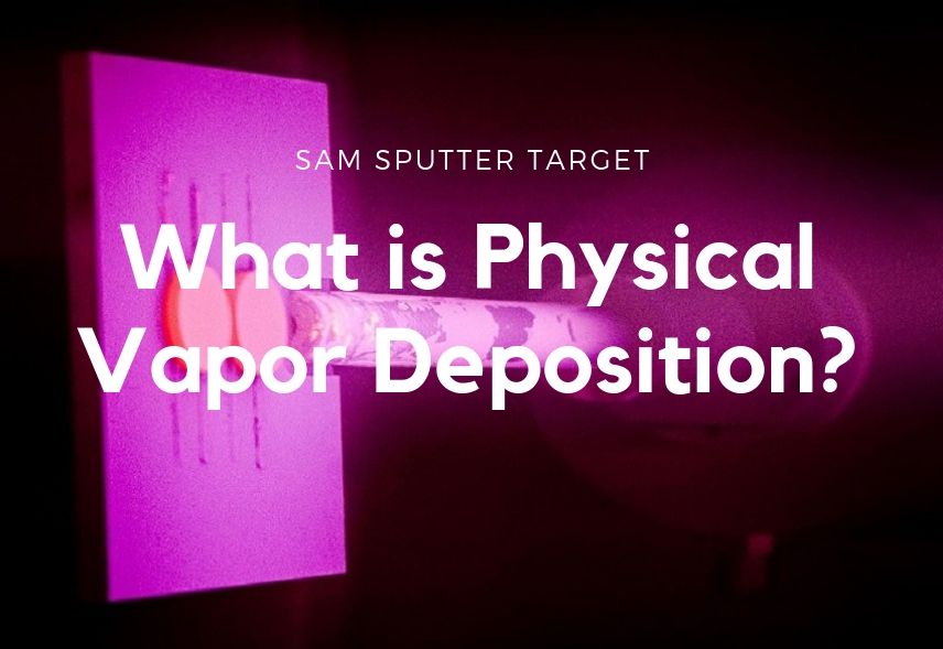
Physical Vapor Deposition (PVD) is a thin film preparation technique that physically vaporizes the surface of a material source (solid or liquid) into gaseous atoms, molecules, or partially ionized into ions under vacuum conditions. Then, a film having a specific function is deposited on the surface of the substrate by a low-pressure gas (or plasma). The main methods of physical vapor deposition include vacuum evaporation, sputtering deposition, arc plasma plating, ion plating, etc. PVD film has fast deposition speed as well as strong adhesion, good diffraction, and a wide application range.
PVD Basic Principles
The process of Physical Vapor Deposition (PVD) can be divided into three fundamental steps:
- Gasification of the Plating Material: The plating material is transformed into a vapor phase through processes such as evaporation, dissociation, or sputtering. This step ensures the material is ready to be deposited onto the substrate.
- Migration of Atoms, Molecules, or Ions: The vaporized atoms, molecules, or ions travel through the vacuum environment. During this phase, various reactions may occur as these particles collide with each other or interact with reactive gases in the chamber.
- Deposition on the Substrate: The vaporized material condenses and adheres to the substrate, forming a thin and uniform coating. The quality and characteristics of the coating depend on factors such as the deposition environment, material properties, and process parameters.
Read more: PVD Thin Film Deposition Materials List
PVD Main Methods:
- Vacuum Evaporation: This method vaporizes materials in a vacuum and deposits them on a substrate to form thin films. It is widely used for microelectronics, thin film resistors, and dielectric coatings. Its simplicity and cost-effectiveness make it suitable for small-scale and research applications.
- Sputtering Deposition: Ions from plasma bombard a target material, ejecting atoms that coat the substrate. Variants like magnetron sputtering and reactive sputtering allow precise control of film composition and thickness. It is extensively used in electronics, solar panels, and reflective coatings.
- Plasma Spray Coating: High-temperature plasma melts materials, which are then sprayed onto substrates, forming robust coatings. This method is ideal for covering large areas and is commonly applied in aerospace for thermal barrier coatings and in medical implants.
- Ion Plating: Vaporized materials are ionized and accelerated towards the substrate, forming dense, highly adherent coatings. This technique is used for durable coatings in cutting tools, automotive trims, and medical instruments.
- Cathodic Arc Deposition: An electric arc vaporizes materials into plasma, which condenses into dense, wear-resistant coatings. It is widely used for tool coatings, decorative finishes, and applications requiring high durability.
- Pulsed Laser Deposition: High-power laser pulses vaporize materials into a plasma plume, which deposits on the substrate. It offers excellent control over film properties and is used in advanced electronics, photovoltaics, and research environments.
- Electron Beam PVD: An electron beam vaporizes high-melting-point materials in a vacuum, producing pure, uniform coatings. It is particularly useful in aerospace for thermal barrier coatings and in optics for anti-reflective layers.
Read more: 7 Main Types of PVD Coating
PVD Advantages
- Excellent Durability: PVD coatings are often harder and more resistant to corrosion compared to traditional methods like electroplating. This makes them ideal for applications requiring long-lasting protection and performance.
- Versatile Applications: PVD can be used with nearly all inorganic and some organic coating materials, offering compatibility with a wide range of substrates and surface finishes. This versatility enables its use in diverse industries and products.
- Environmentally Friendly: Unlike traditional techniques such as electroplating or painting, PVD is conducted in a vacuum, reducing hazardous waste and emissions, making it a more sustainable coating solution.
- Ease of Maintenance: PVD coatings simplify cleaning and maintenance. General copper or gold products coated with PVD require only a soft cloth or glass cleaner for upkeep, saving time and reducing costs.
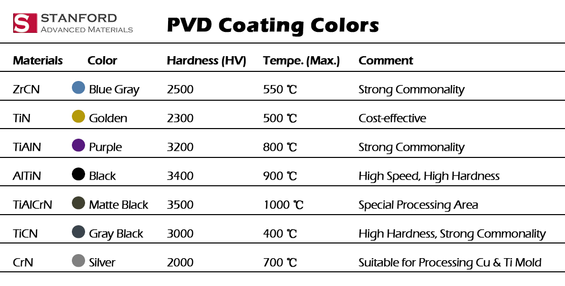
- High Quality with Diverse Options: PVD coatings offer a wide range of colors and finishes, characterized by a smooth surface, rich metallic luster, and resistance to fading. Common colors include golden yellow (TiN), bright silver (CrN), and purple (TiAlN), providing flexibility to meet aesthetic and functional needs.
Read more: Advantages of Physical Vapor Deposition
PVD Applications
Physical Vapor Deposition (PVD) technology stands out for its simplicity, environmental friendliness, and minimal waste production. It creates coatings that are uniform, dense, and strongly bonded to the substrate, making it an ideal choice for a wide range of applications. The advantages of PVD technology have driven its adoption across numerous industries:
- Decorative Applications: PVD is widely used to enhance the appearance and durability of decorative products such as door and window hardware, lamps, jewelry, and handicrafts. The coatings provide vibrant colors, excellent wear resistance, and corrosion protection, ensuring the longevity and aesthetic appeal of these items.
- Cutting Tools and Wear-Resistant Components: PVD coatings are highly valued in the production of cutting tools, molds, and dies. The process improves the hardness and wear resistance of these tools, extending their service life and reducing maintenance costs. Applications in industrial manufacturing, aerospace, and automotive sectors rely on PVD for superior tool performance.
- Medical Devices and Implants: The biocompatibility and precision of PVD coatings make them essential in the medical industry. Surgical instruments, dental tools, and implants benefit from PVD’s ability to provide durable, non-toxic coatings that resist wear and corrosion while ensuring safety in biological environments.
- Electronics and Semiconductors: PVD is a key technology for the electronics industry, used in the deposition of thin films for semiconductors, sensors, and optical components. Its precision and ability to deposit uniform coatings on complex geometries are critical for high-performance electronic devices.
- Aerospace and Automotive: In aerospace, PVD coatings are applied to turbine blades, engine components, and structural parts to enhance thermal resistance and durability. Similarly, in the automotive industry, PVD provides durable, scratch-resistant coatings for trim, emblems, and functional components like piston rings.
- Solar and Energy Industries: PVD technology plays an essential role in manufacturing thin-film solar cells and other energy-related components. It allows for the creation of highly efficient, durable coatings required for energy conversion and storage devices.
PVD Coating Colors
PVD coatings allow for a wide range of colors, such as gold, brass, rose gold, silver white, black, smoky, copper, brown, purple, blue, burgundy, and bronze, applied to materials like stainless steel, copper, and zinc alloy. The resulting coatings are not only visually versatile but also cost-effective compared to pure gold or other metals.
The color variations in PVD coatings are primarily influenced by the thickness of the film, which interacts with light through optical interference. Subtle changes in thickness, especially under one micron, can create different hues. This phenomenon explains why even the same coating material can appear differently depending on the substrate and deposition conditions.
Additionally, PVD coatings provide exceptional properties, such as high hardness, chemical resistance, biocompatibility, and environmental sustainability. For example, combining TiN or ZrN with a gold alloy creates a Titanore PVD coating that meets strict color and quality standards, demonstrating the process’s precision and adaptability.
Read more: PVD Coating: Various Colors Are Available
PVD vs. CVD: What’s the Difference?
Physical vapor deposition (PVD) is a widely used thin film fabrication technique. When it comes to this phrase, many people compare it to chemical vapor deposition (CVD). Although the two phrases differ by only one word, the difference between them is great.
Physical vapor deposition uses physical methods, that is, the transformation of the three states of the substance (gaseous, solid, liquid), so no new substances are produced during the manufacturing process; chemical vapor deposition involves chemical reactions, including the consumption of old materials and the production of new substances. It can be seen that physical vapor deposition has almost no pollution, so in the current “environmentally-friendly” society, physical vapor deposition is increasingly favored by people.
Read more: Table Comparison: Physical Vapor Deposition Vs. Chemical Vapor Deposition
Conclusion
Physical Vapor Deposition (PVD) stands out as a versatile and environmentally friendly thin-film preparation technique, offering unique advantages such as high durability, precision, and adaptability across diverse applications. From enhancing the aesthetics and durability of decorative items to improving the performance of cutting tools, medical devices, and aerospace components, PVD has revolutionized modern manufacturing. Its wide range of available colors and exceptional properties like hardness and corrosion resistance make it a preferred choice in industries where quality and sustainability are paramount.
Stanford Advanced Materials (SAM) is a trusted global supplier of high-quality evaporation material and sputtering target. We offer a comprehensive range of metals, alloys, oxides, and ceramic materials to meet your industrial needs at competitive prices. Stay informed about the latest advancements in PVD and related technologies by visiting our website: https://www.sputtertargets.net. Explore our offerings and discover how we can support your next project with innovative solutions.


