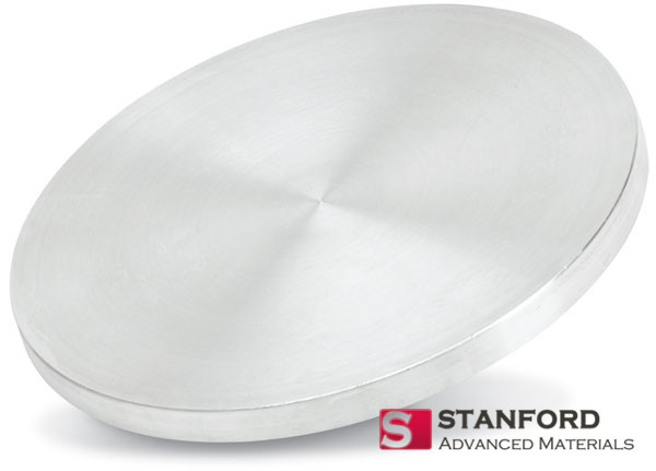
The NbSn Target is a binary alloy designed for sputtering processes, offering a distinctive blend of superconducting, structural, and electrical attributes. Niobium contributes exceptional mechanical strength, a high melting point, and chemical stability, while tin enhances ductility and supports the formation of superconducting intermetallic compounds like NbSn. This target ensures excellent thermal conductivity and reliable performance under high-vacuum and high-energy sputtering conditions. Its finely tuned, homogeneous microstructure—achieved through precise alloying and controlled fabrication methods—guarantees consistent film deposition and uniform composition. The NbSn Target exhibits strong adhesion and compatibility with various substrates, supporting a wide array of thin film deposition techniques. This makes it particularly suitable for producing high-purity superconducting layers, conductive coatings, and functional electronic materials.
Related Products: Niobium Sputtering Target, Nb, Lithium Niobate Sputtering Target, LiNbO3, Tin Sputtering Target, Sn, Tin Zinc Sputtering Target, Sn/Zn
Material Composition: Nb, Sn
Purity: 99.95%
Shape: Planar Disc
Please note that the specifications provided are based on theoretical data. For customized specifications and detailed inquiries, please contact us directly.
Superconducting Films: Ideal for depositing NbSn thin films used in superconducting magnets, quantum computing components, and cryogenic electronics due to their high critical current density and strong tolerance to magnetic fields.
Microelectronics: Utilized in the production of conductive interconnects and barrier layers in microelectronic devices where both structural integrity and electron mobility are essential.
MEMS & Sensors: Applied in micro-electro-mechanical systems (MEMS) and sensitive thin-film sensors that require stable, low-resistance metallic coatings.
Advanced Coatings: Suitable for high-vacuum and high-temperature coatings in scientific instruments or aerospace-grade electronics.
Superconducting RF Cavities: Used in thin-film coatings for accelerator cavities in particle physics research, leveraging the superconducting properties of Nb-Sn compounds.
Our NbSn Targets are meticulously packaged to ensure safety during transit. Depending on the size and dimensions, smaller targets are securely placed in polypropylene (PP) boxes, while larger ones are shipped in custom-built wooden crates. We prioritize tailored packaging solutions and use appropriate cushioning materials to provide maximum protection during transportation.
Packaging Options:

Q1: What is the purity level of the NbSn Target provided by SAM?
A1: Stanford Advanced Materials typically offers NbSn Targets with purity levels of 99.9% or higher. Custom purities are available upon request.
Q2: Which sputtering methods are compatible with NbSn Targets?
A2: NbSn Targets are compatible with both RF and DC magnetron sputtering systems and can be used in high-vacuum or reactive environments, depending on the desired film characteristics.
Q3: How should NbSn Targets be stored?
A3: Targets should be stored in a dry, controlled environment, preferably in vacuum-sealed packaging to prevent oxidation or contamination.
| Property | NbSn Target | Niobium (Nb) Target | Tantalum (Ta) Target |
|---|---|---|---|
| Material Composition | Niobium Tin Alloy | Pure Niobium | Pure Tantalum |
| Applications | Superconductors | Electronics, Alloys | Electronics, Alloys |
| Melting Point | ~2,410°C | ~2,468°C | ~2,996°C |
| Density (g/cm³) | 8.56 | 8.57 | 16.6 |
| Conductivity | Moderate | High | Low |
| Cost | Higher | Moderate | Higher |
| Hardness | Moderate | Moderate | High |
Physical Properties:
Chemical Properties:
Industrial Applications:
Physical Properties:
Chemical Properties:
Industrial Applications: