| Material | Er |
| CAS Number | 7440-52-0 |
| Size | Customized |
| Density | 8.795 g/cm3 |
| Purity | 99.9% |
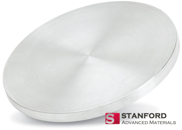
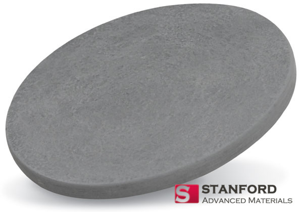
Stanford Advanced Materials (SAM) provides high-purity Erbium Planar Targets, composed of erbium metal with purity levels ranging from 99.9% to 99.99% (3N-4N), specifically designed for high-performance thin-film deposition applications. These targets come in standard sizes from 50 mm to 200 mm in diameter, with thicknesses between 3 mm and 10 mm, and can be customized with bonded backplates (such as Cu or Mo) for enhanced thermal stability, particularly in high-power sputtering systems. With a fine-grain microstructure (<50 µm) and a density greater than 95% of the theoretical value, SAM ensures minimal particle emission and excellent uniformity of the deposited films. To prevent oxidation, all targets are packaged in a vacuum-sealed, argon-filled environment with desiccants, preserving surface quality during storage and shipping. Our rigorous quality control includes ICP-MS impurity analysis, XRD crystallographic testing, and surface roughness measurements (<0.5 µm Ra), all in line with ASTM F3091 and ISO 9001 standards. SAM also provides technical support on sputtering parameters (such as RF power optimization and argon gas pressure ranges) and guarantees delivery within 3-4 weeks for standard orders.
Packaging SAM offers a variety of packaging options based on the product size. Smaller targets are securely packed in PP boxes, while larger ones are shipped in custom wooden crates, all designed to ensure maximum protection during transport.
1. Production Steps:
 2. Quality Testing:
| Feature | Erbium Rotary Target | Erbium Planar Target |
|---|---|---|
| Material Utilization | 80-90% | 30-40% |
| Service Life | Longer | Shorter |
| Coating Uniformity | More uniform | Variability in thickness |
| Production Cost | Higher initial cost | Lower initial cost |
| Applications | Large-area coatings | Small-area coatings |
| Sputtering Stability | Higher | Potentially lower |
| Compatible Equipment | Rotary sputtering systems | Planar sputtering systems |