| Purity | 99.9~99.99%, ≥99.99% |
| Theoretical Density | 4.47 g/cm3 |
| Melting Point | 1526 ℃ |
| Product Shape | Rectangular, or customized upon request |
| Product Size | Customized |
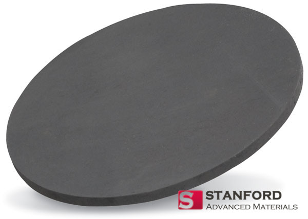
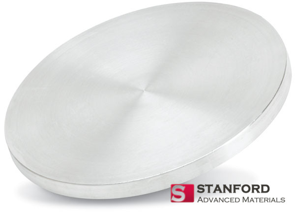
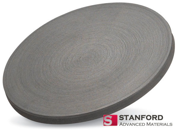
Stanford Advanced Materials (SAM) offers high-purity Yttrium (Y) Planar Targets, designed for high-performance thin-film deposition. Yttrium is a rare-earth metal with a high melting point of 1,522°C, excellent oxidation resistance, and good mechanical strength, making it an ideal material for demanding coating applications. One of yttrium’s key advantages is its ability to form a stable oxide layer, which enhances corrosion resistance and durability, even in high-temperature or reactive environments. Additionally, yttrium provides strong adhesion and uniform film deposition, ensuring high-quality coatings with minimal defects.
SAM supplies yttrium planar targets in various purities (up to 99.999%), sizes, and custom shapes to meet different sputtering system requirements. Our advanced manufacturing process ensures precise composition control, fine-grain structure, and minimal contamination, optimizing sputtering efficiency and film performance. Whether used for specialized coatings or functional thin films, SAM’s yttrium sputtering targets offer superior thermal stability, chemical resistance, and coating uniformity, making them a trusted choice for cutting-edge industries.
| Purity | 99.9~99.99%, ≥99.99% |
| Theoretical Density | 4.47 g/cm3 |
| Melting Point | 1526 ℃ |
| Product Shape | Rectangular, or customized upon request |
| Product Size | Customized |
*The above product information is based on theoretical data. For specific requirements and detailed inquiries, please get in touch with us.
Yttrium planar sputtering targets are widely utilized in advanced thin-film deposition due to their excellent oxidation resistance, high-temperature stability, and strong adhesion properties. Key applications include:
Electronics and Semiconductor Industry: Used as protective and insulating layers in microelectronic devices to enhance durability and performance.
Optical Coatings: Produces high-transparency, anti-reflective, and protective films for lenses, displays, and laser systems.
Superconducting Thin Films: Essential in the development of Yttrium Barium Copper Oxide (YBCO) superconductors, which are crucial for energy-efficient electrical systems and advanced research applications.
Aerospace and Energy Sectors: Applied in thermal barrier coatings to protect components from extreme temperatures and oxidation.
Magnetic Storage and Data Recording: Yttrium-based thin films improve the stability and performance of hard drives and memory devices.
Semiconductor Fabrication Equipment: Utilized in plasma-resistant coatings to enhance the longevity and reliability of fabrication equipment.
Our products are packaged according to their size and specifications. Smaller items are packed in polypropylene (PP) boxes for protection, while larger components are secured in custom wooden crates. Each package is fitted with appropriate cushioning to prevent damage in transit.
Packaging options: Carton, wooden crate, or fully customized.
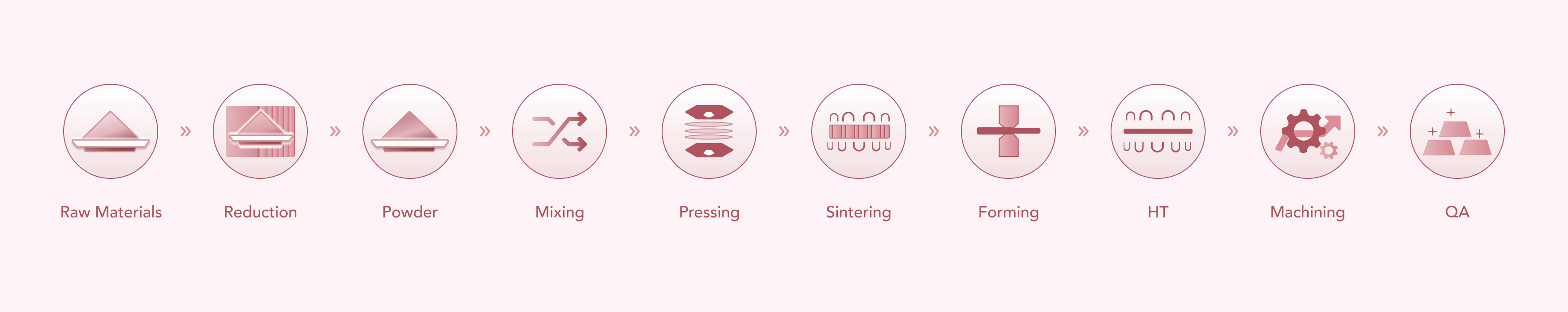
1. Brief Manufacturing Process Flow
 2. Testing Method
Chemical Composition Analysis
Verified using GDMS (Glow Discharge Mass Spectrometry) or XRF (X-ray Fluorescence) to confirm purity and meet material specifications.
Mechanical Properties Testing
Includes tensile strength, yield strength, and elongation tests to evaluate structural performance.
Dimensional Inspection
Measurements of thickness, width, and length are taken to ensure targets fall within specified tolerances.
Surface Quality Inspection
Visual and ultrasonic inspections detect surface defects such as cracks, scratches, or inclusions.
Hardness Testing
Confirms uniformity and mechanical reliability across the target surface.
Q1: What advantages does yttrium offer in thin-film coatings?
A1: Yttrium offers excellent oxidation resistance, thermal stability, and film adhesion. It supports uniform deposition, making it suitable for electronics, optical components, and superconducting materials.
Q2: Can yttrium planar targets be customized?
A2: Yes. We offer custom sizes, shapes, and bonding configurations to match different sputtering systems.
Q3: How should yttrium targets be stored and handled?
A3: Yttrium is reactive to moisture and air. Store in a dry, clean environment and handle with gloves or tools to avoid contamination or oxidation.
Yttrium Rotary Target vs. Yttrium Planar Target
| Feature | Yttrium Rotary Target | Yttrium Planar Target |
|---|---|---|
| Material Utilization | 80–90% | 30–40% |
| Service Life | Longer | Shorter |
| Coating Uniformity | High, suitable for large areas | May vary across surface |
| Cost Efficiency | Higher upfront, better long term | Lower initial, higher replacement frequency |
| Ideal Applications | Displays, solar cells, optics | Semiconductors, precision films |
| Sputtering Stability | More stable, lower material loss | Less stable, prone to uneven erosion |
| Equipment Compatibility | Rotary sputtering systems | Traditional planar systems |
Raw Material: Yttrium (Y)
Atomic Number: 39
Atomic Weight: 88.91
Density: 4.47 g/cm³
Melting Point: 1,522°C (2,772°F)
Boiling Point: 3,345°C (6,053°F)
Thermal Conductivity: ~17 W/m·K
Yttrium is a ductile, silvery-white rare-earth element. It forms a stable oxide layer in air, which protects it from corrosion. Though labeled as a rare-earth metal, yttrium is relatively abundant and is typically sourced from minerals such as xenotime, monazite, and bastnäsite.
Applications:
Superconductors: Key element in YBCO (Yttrium Barium Copper Oxide) high-temperature superconductors.
Optics & Displays: Used in phosphors for CRTs, LEDs, and laser crystals.
Alloys: Improves strength and oxidation resistance in high-performance aerospace materials.
Thin-Film Coatings: Provides durable, stable layers in electronic and optical devices.
Yttrium’s thermal and chemical stability makes it essential for advanced coatings and electronic materials.