| Density | ≥10.15 g/cm3 |
| Average Grain Size | ≤100 um |
| Roughness | ≤0.8 um |
| Flatness | ≤0.30 mm |
| Bonding Rate | ≥98% |
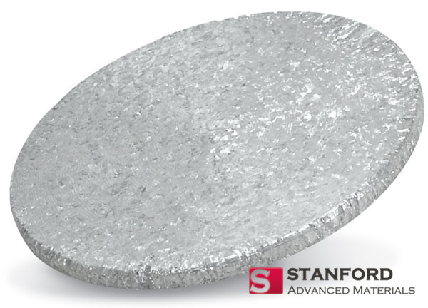
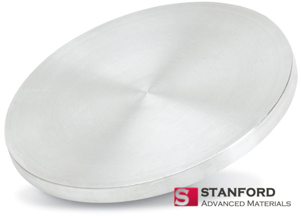
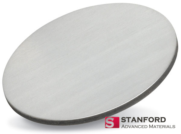
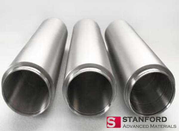
Stanford Advanced Materials (SAM) supplies high-purity molybdenum rotary targets for thin-film deposition in applications like flat panel displays, solar cells, and optical coatings. These targets are made from high-grade molybdenum to ensure strong electrical conductivity, thermal stability, and consistent film formation.
Rotary targets offer better material utilization than planar types, which extends their operational lifespan and lowers production costs. Molybdenum’s high melting point and thermal conductivity make it a solid choice for coating processes that involve high temperatures and vacuum environments.
SAM provides rotary targets in a range of sizes and specifications, tailored for different sputtering systems. With tight process controls and quality standards, SAM’s targets offer consistent performance and support efficient thin-film production.
Properties
| Density | ≥10.15 g/cm3 |
| Average Grain Size | ≤100 um |
| Roughness | ≤0.8 um |
| Flatness | ≤0.30 mm |
| Bonding Rate | ≥98% |
Chemical Composition. %
| Main Content,
%, min |
Mo | 99.95 | 99.97 |
| Impurity Content
(mass fraction), %, max |
Al | 0.0050 | 0.0010 |
| Ca | 0.0020 | 0.0020 | |
| Cr | 0.0100 | 0.0020 | |
| Cu | 0.0020 | 0.0020 | |
| Fe | 0.0050 | 0.0020 | |
| K | – | 0.0020 | |
| Mg | 0.0020 | 0.0010 | |
| Na | – | 0.0010 | |
| Ni | 0.0050 | 0.0010 | |
| Si | 0.0050 | 0.0020 | |
| W | 0.0300 | 0.0300 | |
| S | 0.0050 | – | |
| Cd | 0.0001 | – | |
| C | 0.0100 | 0.0030 | |
| O | 0.0080 | 0.0040 | |
| N | 0.0030 | 0.0010 |
*The above product information is based on theoretical data. For specific requirements and detailed inquiries, please get in touch with us.
Size (mm)
| Rotary |
G6 |
φ135/167*2158 |
|
G8.5 |
φ135/167*2692 |
*Customized sizes are also available upon request. Feel free to contact us for details.
Other shapes: Molybdenum Sputtering Target, Planar Molybdenum (Mo) Sputtering Target
Related Products: Molybdenum Rhenium Sputtering Target, Molybdenum Disilicide Sputtering Target, Molybdenum Silicon Sputtering Target, Molybdenum Selenide Sputtering Target, Molybdenum Boride Sputtering Target
Flat Panel Displays (TFT-LCD & OLED): Used in thin-film transistors for high conductivity and thermal stability.
Solar Cells (CIGS & Thin-Film): Serves as a back-contact layer, improving efficiency and lifespan.
Optical Coatings: Used for anti-reflective and conductive layers in optics and electronics.
Semiconductors: Acts as a barrier and interconnect material in chip fabrication.
Touch Panels: Alloys like MoNb are used for corrosion-resistant sensor electrodes.
Smaller parts are packed in polypropylene boxes.
Larger targets are crated in custom wooden boxes with protective cushioning.
Packaging is tailored to the product’s size and transit requirements.
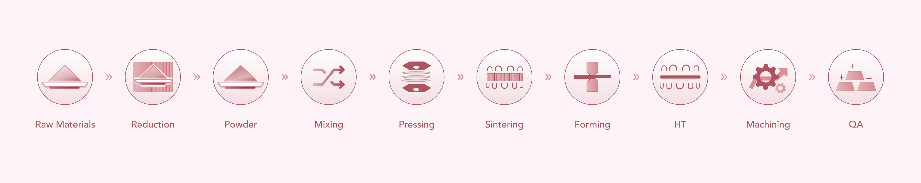
1. Brief Manufacturing Process Flow
2. Testing Method
Chemical Analysis: GDMS or XRF for purity.
Mechanical Testing: Tensile strength, yield, elongation.
Dimensional Inspection: Ensures specs are met.
Surface Quality Check: Visual and ultrasonic inspection for defects.
Hardness Testing: Verifies material integrity.
Q1: Why choose rotary targets over planar?
A1: They use more of the material (up to 80–90%) and last longer, which cuts down on replacements and waste. Further reading: Planar Targets VS. Rotatory Targets
Q2: What industries use these targets?
A2: Common in displays, solar energy, semiconductors, optics, and touchscreens.
Q3: Can these be customized?
A3: Yes. SAM offers custom sizes, thicknesses, and bonding formats to match different sputtering systems.
Molybdenum Rotary Target vs. Molybdenum Planar Target
| Feature | Rotary Target | Planar Target |
|---|---|---|
| Material Utilization | 80–90% | 30–40% |
| Service Life | Longer | Shorter |
| Coating Uniformity | More uniform | May vary |
| Long-term Cost | Lower | Higher |
| Applications | Large-area coatings | Small-area coatings |
| Sputtering Stability | More stable | Less stable |
| Equipment Needed | Rotary systems | Traditional systems |
Molybdenum (Mo) is a refractory metal with a melting point of 2,617°C. It offers high conductivity and resists corrosion under extreme temperatures, which makes it a reliable material across advanced industrial applications.
Key Data:
Atomic Number: 42
Density: 10.28 g/cm³
Thermal Conductivity: 138 W/m·K
Common Uses:
Thin-Film Coating: Displays, solar panels, semiconductors
High-Temp Alloys: Aerospace, power systems
Energy Sector: Nuclear and thermal power
Metallurgy: Steel strengtheners and corrosion-resistant alloys
Catalysis: Petroleum refining and chemical processing