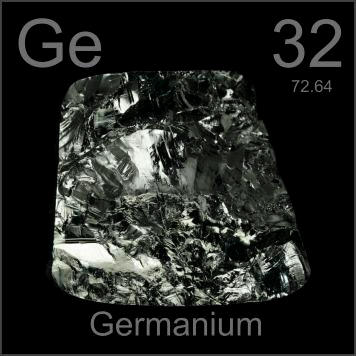
Chemical Formula: Ge
Catalog Number: ST0016
CAS Number: 7440-56-4
Purity: >99.99%, 99.999%
Shape: Discs, Plates, Column Targets, Step Targets, Custom-made
Germanium sputtering target is available in various forms, purities, sizes, and prices. Stanford Advanced Materials (SAM) is a trusted sputtering target supplier working with international partners to bring you the highest quality products with the most affordable pricing.
 Germanium sputtering target is composed of high purity Germanium metal. Germanium is a chemical element originated from Germany (with the Latin name Germania). It was first mentioned in 1886 and observed by A. Winkler. “Ge” is the canonical chemical symbol of germanium. Its atomic number in the periodic table of elements is 32 with location at Period 4 and Group 14, belonging to the p-block. The relative atomic mass of germanium is 72.64(1) Dalton, the number in the brackets indicating the uncertainty.
Like silicon, germanium is a semiconductor and frequently utilized in the fabrication of transistors and integrated circuits. It is often evaporated under vacuum to create layers in the production of optical storage media and optical coatings. Other uses of the material are as an alloying agent and catalyst.
| Material Type | Germanium |
| Symbol | Ge |
| Color/Appearance | Grayish White, Semi-Metallic |
| Melting Point | 973 °C |
| Sputter | RF, DC |
| Density | 5.32 g/cc |
| Thermal Conductivity | 60 W/m.K |
| Type of Bond | Indium |
| Available Sizes | Dia.: 1.0″, 2.0″, 3.0″, 4.0″, 5.0″, 6.0″ Thick: 0.125″, 0.250″ |
Indium Bonding is available recommended for germanium sputtering target, due to some of its characteristics not amenable to sputtering like brittleness, low thermal conductivity. Stanford Advanced Materials is devoted to machining standard backing plates and working together with the Taiwan Bonding Company for providing bonding services. For questions about target bonding materials, methods and services, please click here.

SAM’s germanium sputtering targets are available in various forms, purities, sizes, and prices. We specialize in producing high purity thin film deposition materials with the highest possible density and smallest possible average grain sizes for use in semiconductor, chemical vapor deposition (CVD) and physical vapor deposition (PVD) display and optical applications. Please send us an inquiry for current pricing on sputtering targets and other deposition materials not listed.
Submit your review | |
1 2 3 4 5 | |
Submit Cancel | |
Bought these and donated them to the local Community College chemistry lab.
Hope they be happy when they are to receive these gift.