Chemical Formula: Er
Catalog Number: ST0013
CAS Number: 7440-52-0
Purity: 99.9%
Shape: Discs, Plates, Column Targets, Step Targets, Custom-made
The erbium sputtering target is available in various forms, purities, sizes, and prices. Stanford Advanced Materials (SAM) is a trusted sputtering target supplier working with international partners to bring you the highest quality products.
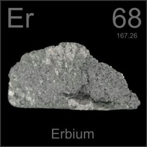
 The erbium sputtering target is composed of high purity erbium metal. Erbium is a chemical element that originated from Ytterby, Sweden. It was first mentioned in 1842 and observed by G. Mosander. “Er” is the canonical chemical symbol of erbium. Its atomic number in the periodic table of elements is 68 with a location at Period 6 and Group 3, belonging to the f-block. The relative atomic mass of erbium is 167.259(3) Dalton, the number in the brackets indicating the uncertainty.
Read more: Erbium Rare Earth Element: Introduction, Properties, and Applications
| Material Type | Erbium |
| Symbol | Er |
| Color/Appearance | Silvery White, Metallic |
| Melting Point | 1,412 °C |
| Thermal Conductivity | 15 W/m.K |
| Density | 9.05 g/cc |
| Sputter | DC |
| Coefficient of Thermal Expansion | 12.2 x 10⁻⁶/K |
| Available Sizes | Dia.: 2.0″, 3.0″, 4.0″, 5.0″, 6.0″ Thick: 0.125″, 0.250″ |
We also offer other customized shapes and sizes of the sputtering targets, please send us an inquiry for more information.
1. No bonding service is presently available for the erbium sputtering target. 2. This material has high chemical activity when exposed to the environment. Oil packaging and clean procedure are required to prevent it from chemical reactions.
The erbium sputtering target is clearly tagged and labeled externally to ensure efficient identification and quality control. Great care is taken to avoid any damage which might be caused during storage or transportation.
SAM’s erbium sputtering targets are available in various forms, purities, sizes, and prices. We specialize in producing high purity thin film deposition materials with the highest possible density and smallest possible average grain sizes for use in semiconductor, chemical vapor deposition (CVD) and physical vapor deposition (PVD) display and optical applications. Please send us an inquiry for the current prices of sputtering targets and other deposition materials that are not listed.
Submit your review | |
1 2 3 4 5 | |
Submit Cancel | |
Feel happy that I could get these high-quality products for such a great price! Worked great for my project.