Chemical Formula: Au/Sn
Catalog Number: ST0487
Purity: 99.99%
Shape: Discs, Plates, Column Targets, Step Targets, Custom-made
The Gold Tin Sputtering Target is available in various forms, purities, sizes, and prices. Stanford Advanced Materials (SAM) offers high-quality sputtering targets at the most competitive prices.
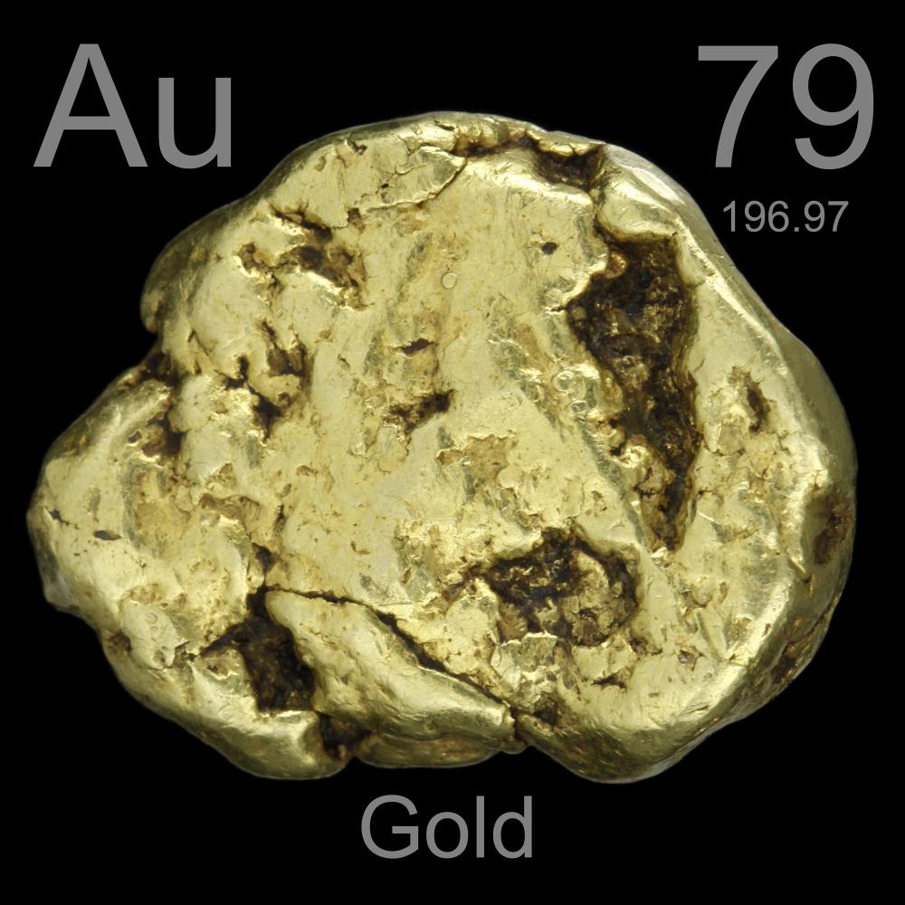
 Gold is a chemical element that originated from the Anglo-Saxon word gold (aurum in Latin, meaning glow of sunrise). It was early used before 6000 BC and discovered by people from the Middle East. “Au” is the canonical chemical symbol of gold. Its atomic number in the periodic table of elements is 79 with a location at Period 6 and Group 11, belonging to the d-block. The relative atomic mass of gold is 196.966569(4) Dalton, the number in the brackets indicating the uncertainty.
 Tin, also called stannum, is a chemical element that originated from the Anglo-Saxon word tin (stannum in Latin, meaning hard). It was early used in 3500 BC. “Sn” is the canonical chemical symbol of tin. Its atomic number in the periodic table of elements is 50 with location at Period 5 and Group 14, belonging to the p-block. The relative atomic mass of tin is 118.710(7) Dalton, the number in the brackets indicating the uncertainty.
Related Products: Gold Sputtering Target, Tin Sputtering Target, Alloy Sputtering Targets
| Material Type | Gold Tin |
| Symbol | Au/Sn |
| Color/Appearance | Solid |
| Melting Point | 2100 °C |
| Density | N/A |
| Available Sizes | Dia.: 2.0″, 3.0″, 4.0″, 5.0″, 6.0″ Thick: 0.125″, 0.250″ |
We also offer other customized shapes and sizes of the sputtering targets, please send us an inquiry for more information.
Our Gold Tin Sputtering Targets are clearly tagged and labeled externally to ensure efficient identification and quality control. Great care is taken to avoid any damage which might be caused during storage or transportation.
SAM’s Gold Tin Sputter Targets are available in various forms, purities, sizes, and prices. We specialize in producing high-purity physical vapor deposition (PVD) materials with the highest possible density and smallest possible average grain sizes for use in semiconductor, chemical vapor deposition (CVD), and physical vapor deposition (PVD) display and optical applications. Get an inquiry right now.
Submit your review | |
1 2 3 4 5 | |
Submit Cancel | |
I bought these for chemistry class to do some film coating experiments with. They function properly for what we use them for.