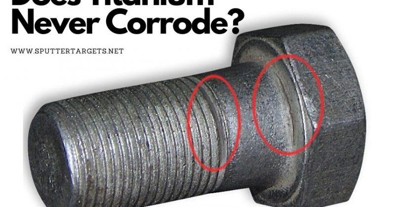
(949) 407-8904 Mon - Fri 08:00 - 17:00 23661 Birtcher Dr., Lake Forest, California, USA

Company Dynamic

Platinum vs. Gold Ring

Platinum vs. Gold: Which Material Is Better for Rings?

As for the two most commonly used metals for engagement and wedding rings, platinum and gold, most people distinguish them by their different colors-platinum is naturally white, and gold is naturally yellow. However, rings made of white gold (composed of gold, alloys, and a rhodium plating) have a similar white color to platinum rings. Since...
Continue Reading
An Overview of Tantalum Element

An Overview of Tantalum Element

Tantalum Overview The texture of the tantalum is very hard and the hardness can reach 6-6.5. Its melting point is as high as 2996 °C, only after carbon, tungsten, rhenium, and osmium. Tantalum is malleable and can be drawn into a thin foil. Its coefficient of thermal expansion is very small, and it only expands by 6.6 parts...
Continue Reading
Sputter Coating Technologies Direct Current Sputtering

Sputter Coating Technologies: Direct Current Sputtering (DC Sputtering)

We have previously made a brief introduction of Five Sputter Coating Technologies, including unbalanced magnetron sputtering, radio frequency sputtering (RF sputtering), direct current magnetron sputtering (DC sputtering), mid-frequency alternating current magnetron sputtering (AC sputtering), and reactive magnetron sputtering. In this article, we are going to talk about direct current (DC) sputtering in detail. To begin...
Continue Reading
sputtering target for electronics

Types and Applications of Sputtering Targets in the Electronic Industry

Sputtering targets have important applications in many areas, such as architecture, optics, electronics and so on. Sputtering targets used in electronic industry can be subdivided into semiconductor target (also called anelva target), planar target, coated glass target, solar photovoltaic target, and so on. There are some differences in the selection and performance requirements of sputtering materials in different application fields....
Continue Reading

How is the Semiconductor Wafer Manufactured? (With Infographic)

Semiconductor wafers are the basic material for manufacturing electronic chips. The most important raw material for semiconductor integrated circuits is silicon, which is widely found in rocks and gravels in the form of silicates or silica in nature. The fabrication process of the semiconductor silicon wafer can be divided into three basic steps: silicon purification...
Continue Reading

What Are the Applications of Sputtering Targets? (With Video)

Sputtering targets are a physical vapor deposition (PVD) mechanism with many uses in modern technology and manufacturing. In the sputtering process, the atoms are pulled from the sputter target with powerful magnets, and a controlled gas (usually argon) is introduced. Then, the processed to collide with each other in their gaseous state before condensing into...
Continue Reading
1 25 26 27 28 29 42