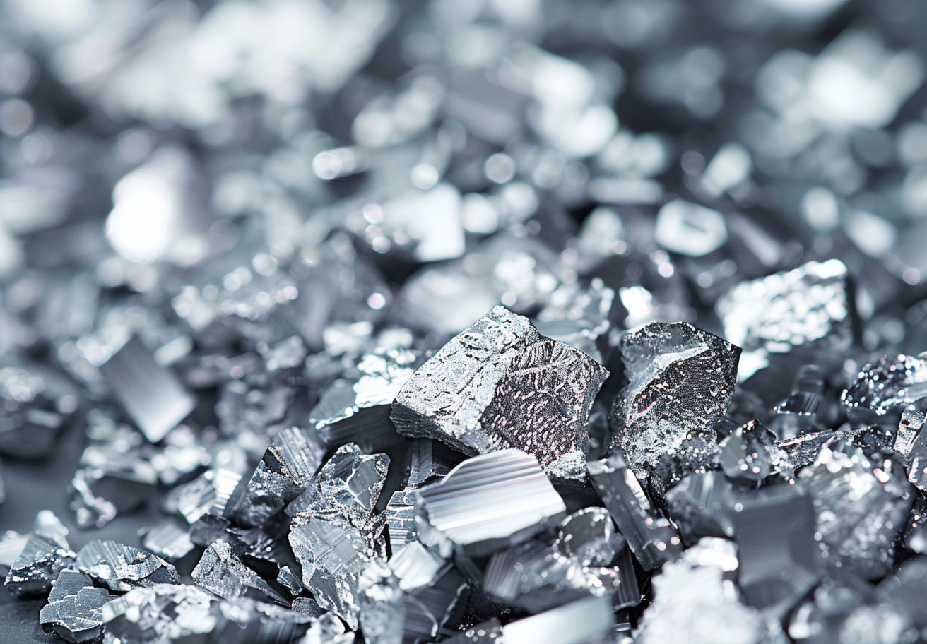
The insatiable requirement for thinner, faster, and power-saving technologies has made the semiconductor industry one of the prime drivers of technological advancement. Behind the drive is a critical material: high-purity tantalum (Ta) sputtering targets. The targets are a critical ingredient in enabling next-generation semiconductor manufacturing processes, solving dire issues to chip reliability and performance. Tantalum...Continue Reading
1. Introduction Refractory metals like tantalum (Ta) and niobium (Nb) play an increasingly important role in thin film technology, particularly for environments that demand both high-temperature stability and corrosion resistance. These two elements, known for their exceptionally high melting points and strong chemical inertness, have found widespread use in advanced protective coatings. As industries such...Continue Reading
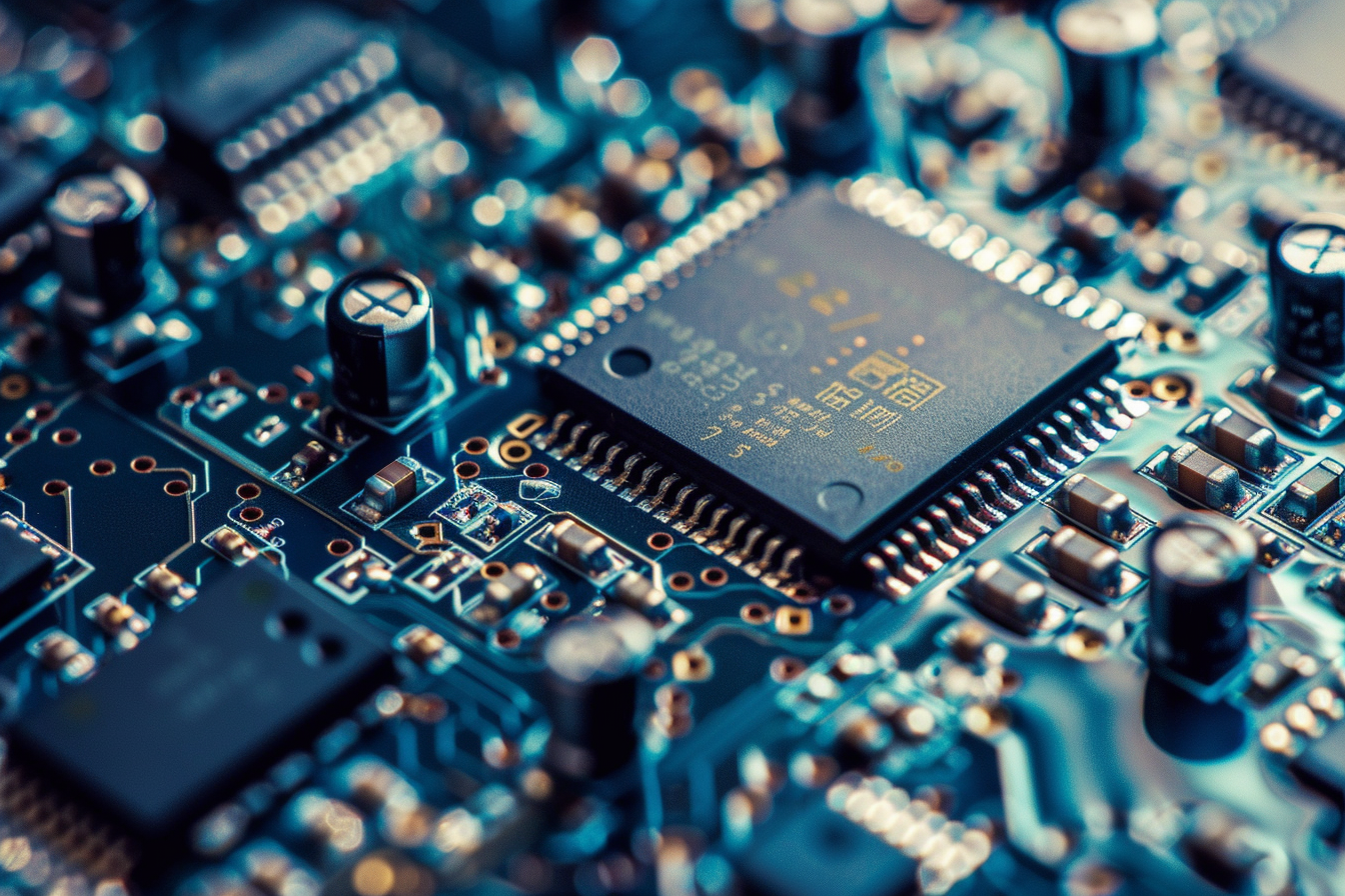
When we think about semiconductor manufacturing, we often picture highly advanced technologies, intricate processes, and an army of materials working in the background. Among these materials, tantalum (Ta) sputtering targets play a surprisingly crucial role. But why exactly is this unassuming metal so important for semiconductor devices? Let’s dive in. What Makes Tantalum So Special...Continue Reading
1. Introduction to PVD and CVD Physical vapor deposition (PVD) and chemical vapor deposition (CVD) are two essential thin-film deposition techniques widely used in semiconductors, tooling, optics, and clean energy. PVD relies on physical transformation (solid to vapor to solid), while CVD creates coatings through chemical reactions on the substrate surface. 2. Technical Comparison Table...Continue Reading
I. Introduction High-entropy alloys (HEAs) represent a paradigm shift in alloy design. Unlike traditional alloys that rely on a dominant elemental component, HEAs are composed of five or more principal elements in near-equiatomic or equimolar ratios. This unique composition results in high-entropy solid solutions with superior properties not achievable by conventional alloys. The concept of...Continue Reading
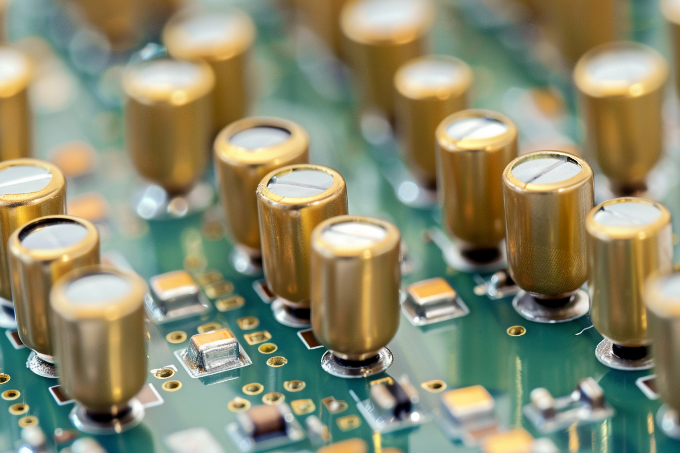
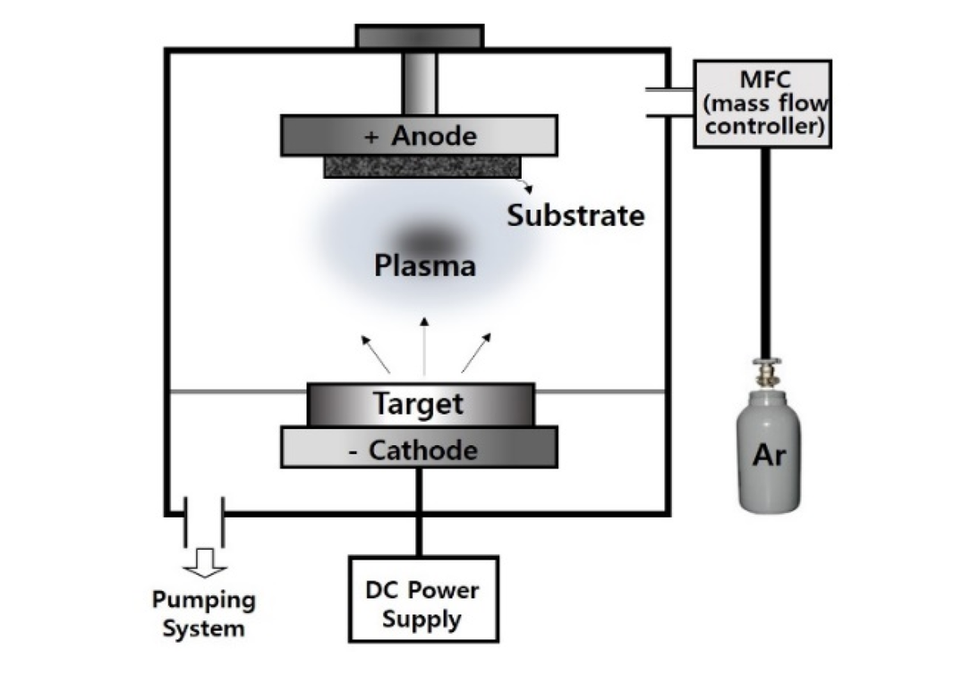
Introduction Background of Sputtering Technology Thin film deposition is a cornerstone in the fabrication of modern technological devices. From electronic components to optical coatings, the demand for high-quality thin films has surged, driving advancements in deposition techniques. Among these, sputtering has emerged as a versatile and reliable method, offering precise control over film composition and...Continue Reading
Since ancient times, gold has been revered as a highly valuable material. From making jewelry to cookware and industrial materials, gold has proven to be very useful and precious to man, particularly because of its high malleability, ductility, and lustrous nature. Gold is one of the most precious metals known to man, and it has...Continue Reading
Physical Vapor Deposition (PVD) is a widely used technique in various industries, such as electronics, optics, and materials science. It is crucial for depositing thin films onto substrates, which are essential in the manufacturing of components like semiconductors, mirrors, and solar panels. The quality, thickness, adhesion, and performance of the thin film depend largely on...Continue Reading
I. Introduction Silicon-on-insulator (SOI) technology represents a pivotal advancement in semiconductor manufacturing, offering enhanced performance and efficiency over traditional bulk silicon approaches. By integrating a thin silicon layer atop an insulating substrate, SOI facilitates superior electrical isolation and reduced parasitic capacitance, which is critical for high-performance electronic devices. SOI involves layering a silicon wafer on...Continue Reading