Introduction to PVD Coatings Physical Vapor Deposition (PVD) stands at the forefront of surface coating technologies, widely embraced by industries such as watches, jewelry, and automotive for its profound impact on product durability, aesthetics, and performance. This method distinguishes itself through its ability to offer coatings that are not only remarkably hard and corrosion-resistant but...Continue Reading
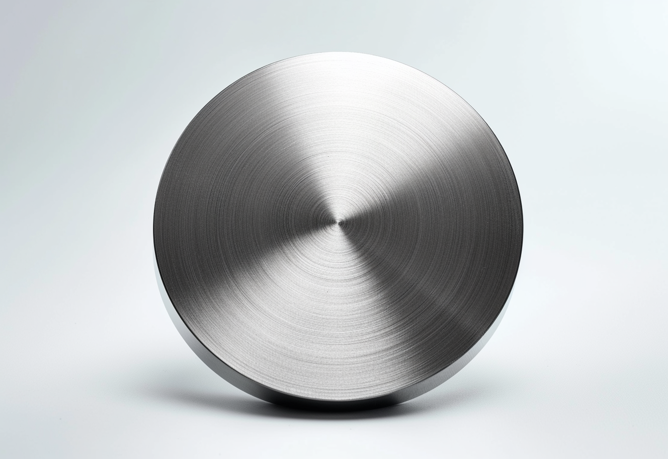
Introduction to Molybdenum Sputter Targets In the realm of material science and thin-film technology, molybdenum sputter targets hold a pivotal position. These targets, crafted from molybdenum, a transition metal known for its high melting point and remarkable thermal and electrical conductivity, are instrumental in the physical vapor deposition (PVD) process. This process is critical for...Continue Reading
In the ever-evolving landscape of technology and materials science, certain elements stand out for their unique properties and critical roles in advancing innovation. Germanium is one such element, a cornerstone in the development of cutting-edge technologies across a wide range of industries. This comprehensive guide delves into the world of Germanium Sputter Targets, exploring their...Continue Reading
In the world of advanced materials and cutting-edge technology, Ytterbium Sputter Targets have emerged as crucial components in various applications, ranging from electronics to optics. These targets play a pivotal role in the sputtering process, a key technique in thin film deposition. In this article, we will delve into the fascinating realm of Ytterbium Sputter...Continue Reading
Introduction In the realm of thin-film deposition technologies, Palladium Sputter Targets have emerged as key components, shaping advancements in various industries. This comprehensive guide aims to provide an in-depth understanding of Palladium Sputter Targets, covering their properties, manufacturing processes, and wide-ranging applications. Properties of Palladium Sputter Targets Palladium, a transition metal belonging to the platinum...Continue Reading
Introduction In the realm of advanced materials and cutting-edge technologies, cobalt sputter targets have emerged as key players, revolutionizing various industries. This article aims to delve into the intricacies of cobalt sputtering targets, exploring their applications, manufacturing process, and significance in the world of thin-film deposition. Understanding Cobalt Sputter Targets Cobalt sputter targets are vital...Continue Reading
Introduction Platinum sputtering targets, often referred to as Pt sputter targets, play a crucial role in various industries, including electronics, optics, and materials science. This will cover everything you need to know about platinum sputtering targets. It will include their uses, how they are made, and the advantages they offer in different areas. Applications...Continue Reading
If you’ve ever wondered about the magic behind the shiny surfaces of electronic devices, solar cells, or even reflective mirrors, you might find the answer in a small but crucial component: the silver sputter target. In this article, we’ll break down the basics of silver targets, exploring what they are, how they work, and the...Continue Reading
Aluminum sputtering targets play a crucial role in the world of thin film technology, finding versatile applications across various industries. In this article, we’ll delve into the diverse uses of aluminum sputter targets, exploring how they contribute to the creation of thin films that impact our daily lives. Introduction Aluminum sputtering targets, often overlooked in...Continue Reading