Introduction Thin-film deposition techniques play a crucial role in various industries, providing protective coatings that enhance the properties of materials. Among these methods, Physical Vapor Deposition (PVD) and Chemical Vapor Deposition (CVD) stand out, each distinguished by their unique characteristics, including the temperature at which they operate. Temperature Difference in PVD Definition and Basic Principles PVD encompasses...Continue Reading
Introduction Physical Vapor Deposition (PVD) technology is at the forefront of materials science, continually evolving to meet the demands of various industries. In this article, we undertake a comprehensive exploration of the evolving trends in PVD technology. From the latest innovations to potential applications across different industries, we delve into the intricate landscape of PVD....Continue Reading
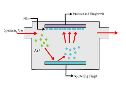
Introduction Thin film coatings are a critical component of various industries, from microelectronics to optics. Two prominent techniques for depositing these thin films are sputtering and thermal evaporation. Let’s compare these two technologies to understand their strengths and applications. Sputtering: Precision and Versatility Sputtering is a physical vapor deposition (PVD) technique that involves the removal...Continue Reading
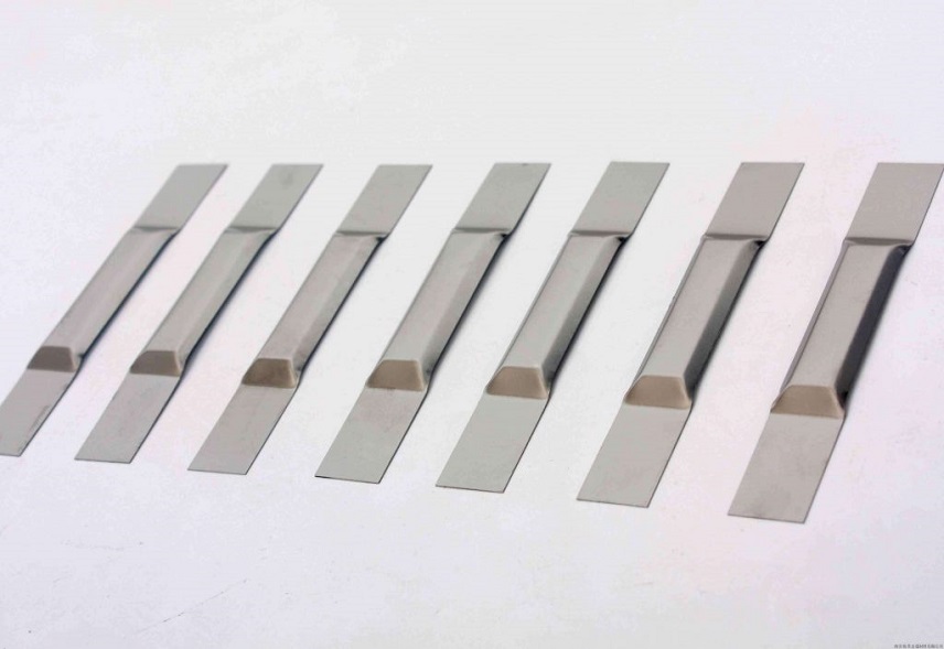
Introduction Molybdenum boats, often crafted from high-purity molybdenum material, are versatile tools with a wide range of applications across various industries. These boat-shaped containers are valued for their exceptional heat resistance, high melting point, and robustness. In this article, we’ll explore the uses and material properties of molybdenum boats, shedding light on their importance in...Continue Reading
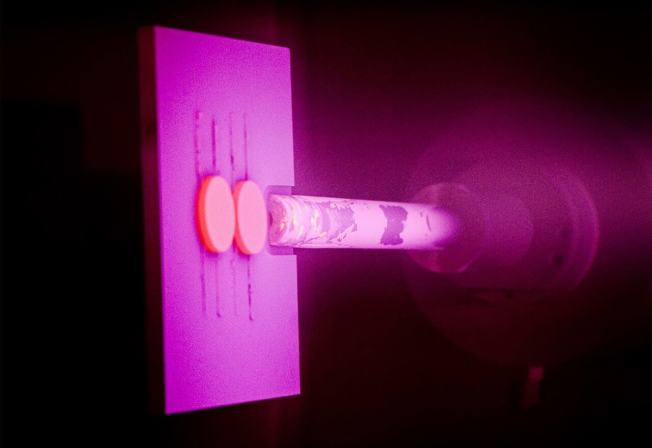
Introduction Sputtering is a cornerstone of physical vapor deposition (PVD) and stands at the forefront of materials science and advanced manufacturing. This versatile technique plays a pivotal role in the deposition of thin films onto substrates with plenty of advantages and limitations. In this article, we will delve into the world of sputtering, uncovering its...Continue Reading
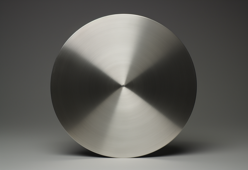
Introduction Sputtering is a common thin-film deposition technique used in various industries, including semiconductors, optics, and surface coatings. A sputtering target is a key component in the process, as it is responsible for generating the material to be deposited onto a substrate. It is important to ensure that the sputtering target is used at a...Continue Reading
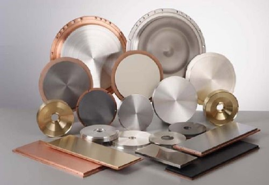
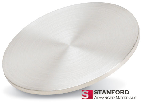
Introduction Palladium (Pd) is a highly sought-after metal for thin film deposition due to its unique properties. One popular method for depositing Pd thin films is through the use of sputtering targets. In this article, we will explore the benefits of using palladium sputter targets for thin film deposition and their applications in various...Continue Reading
Introduction Gallium Arsenide (GaAs) wafers have a variety of applications in the field of electronics, particularly in the production of high-performance electronic devices. In this article, we will explore some common applications of GaAs wafers for electronic device manufacturing and provide a better understanding of their properties and advantages. Properties of Gallium Arsenide Wafer Gallium...Continue Reading
Introduction The deposition rate is an important factor in the field of thin film deposition, as it directly affects the production efficiency and throughput of the process. In this article, we will discuss practical methods to increase the deposition rate for various deposition techniques. Hope that you can have a better understanding of the factors...Continue Reading