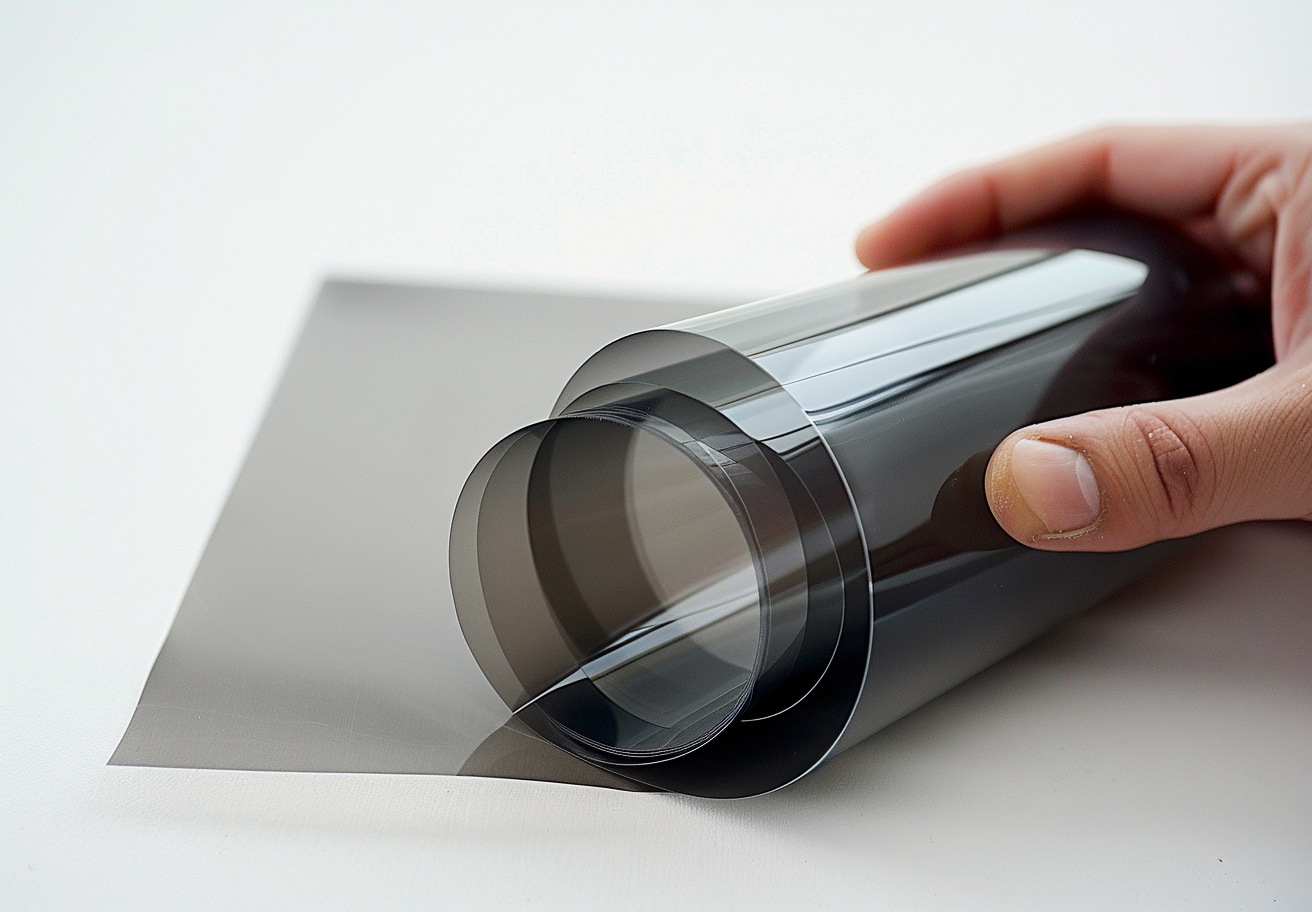
1. Introduction Transparent Conductive Oxides (TCOs) are a unique class of materials that combine two essential properties: optical transparency and electrical conductivity. These characteristics make TCOs indispensable in various technological applications, ranging from touch screens and flat-panel displays to solar cells and smart windows. The ability to conduct electricity while allowing light to pass through...Continue Reading
Transparent conductive oxides (TCOs) are materials that possess the unique combination of being both electrically conductive and optically transparent. These materials are critical in a variety of modern technologies, including displays, solar cells, and touch screens. Among the most widely used TCOs are Indium Tin Oxide (ITO) and Fluorine-doped Tin Oxide (FTO). This article explores...Continue Reading
Introduction Physical Vapor Deposition (PVD) and Chemical Vapor Deposition (CVD) are prominent coating processes used in various industries to enhance the surface properties of materials. These processes provide protective and functional coatings that improve hardness, wear resistance, and other surface characteristics. This article provides an extensive comparison between PVD and CVD, delving into their mechanisms,...Continue Reading
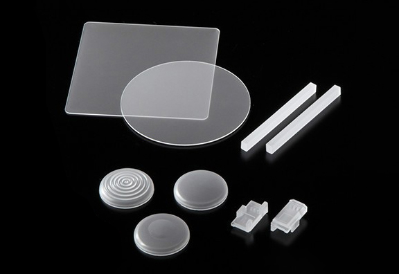
Introduction In the realm of semiconductor manufacturing, the choice of substrate material is critical, directly impacting the performance and durability of the end product. Semiconductor substrates serve as the foundational layer for the deposition of various electronic circuits, and their material properties can significantly influence the efficiency and functionality of these devices. Among the various...Continue Reading
Introduction Synthetic diamonds, particularly those produced by Chemical Vapor Deposition (CVD), represent a significant technological advancement that blends centuries of curiosity and modern scientific ingenuity. Historically, diamonds have been highly sought after not only for their aesthetic value but also for their remarkable physical properties. Researchers like Isaac Newton have studied these properties, paving the...Continue Reading
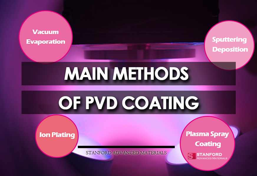
Introduction Physical Vapor Deposition (PVD) is a critical technique used extensively in the manufacturing industry to enhance the surface properties of materials. This process involves the deposition of thin films of material onto various substrates, which can include metals, glass, ceramics, and plastics. PVD is celebrated for its ability to significantly improve the hardness, wear...Continue Reading
Thin-film transistors (TFTs) are fundamental components in a myriad of electronic devices that shape our daily lives, from the vibrant displays of smartphones and TVs to the essential functionality of touch screens and solar cells. Central to the fabrication of these versatile transistors is the use of magnesium oxide (MgO) targets, a critical material in...Continue Reading
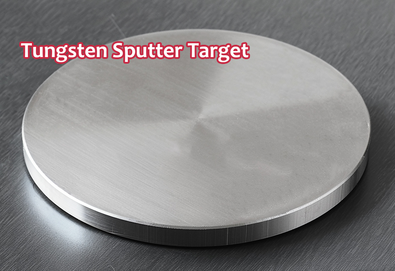
Introduction Sputter deposition, a pivotal technique in thin-film coatings, utilizes physical vapor deposition (PVD) to create material films on various substrates. Among the materials used for sputter targets, tungsten stands out due to its significant properties and applications in various high-tech industries. This article delves into the world of tungsten sputter targets, exploring their characteristics,...Continue Reading
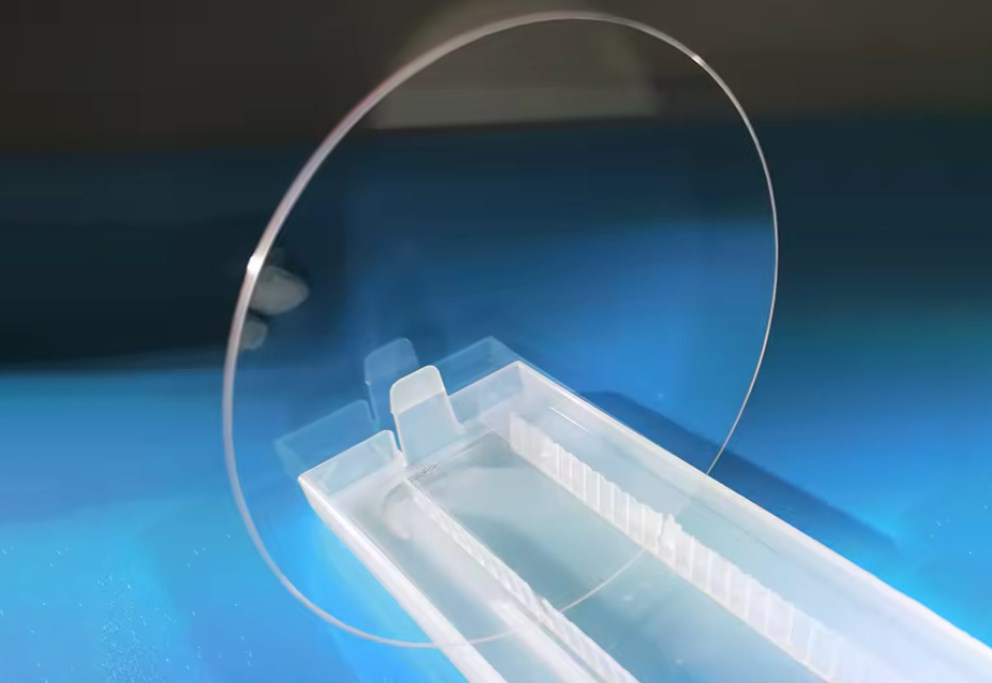
Introduction Chemical Vapor Deposition (CVD) is a pivotal technology in the field of material science, enabling the synthesis of high-performance materials under controlled conditions. This technique involves the deposition of a material’s vapor phase onto a substrate, forming thin films or structures with precise compositional and structural properties. Among the myriad of materials synthesized using...Continue Reading