Ion Beam Sputtering Definition Ion beam sputtering (IBS), or ion beam deposition (IBD), is a thin film deposition technology that uses an ion source to deposit a sputtering target onto a substrate to produce the highest quality films with excellent precision. Compared to other PVD technologies, ion beam sputtering is more accurate and can accurately control...Continue Reading
What is Sputtering Deposition? Sputtering deposition, or sputter coating, is one of the physical vapor deposition technology, whereby particles are ejected from a solid target material due to the bombardment of the target by energetic particles. It is an electronic process that deposits thin films of metals or other materials onto a variety of surfaces. Most often,...Continue Reading
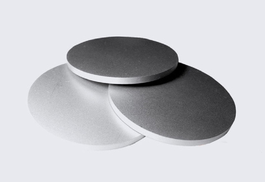
The sputtering target is an important material for physical vapor deposition, the most widely used technology for depositing materials. As its name suggests, “physical” means that the PVD coating method involves a purely physical process. During the physical vapor deposition, a solid target material is broken up into the vapor state (usually in a high...Continue Reading
Magnetron sputtering is a physical vapor deposition method that allows the deposition of various materials, including metals, oxides, ceramics and etc. by using a specially formed magnetic field applied to a diode sputtering target. The deposition rate, or the film formation rate, is an important parameter that measures the effectiveness of the magnetron sputtering machine....Continue Reading
An Overview of Magnetron Sputtering Magnetron sputtering, a physical vapor deposition (PVD) process, is a main thin film deposition method for manufacturing semiconductors, disk drives, CDs, and optical devices. Magnetron sputtering has the advantages of high speed, low temperature, and low damage. In this article, let’s take a look at the definition, working principle, and...Continue Reading
What are the Three Generations of Semiconductor Materials? The first generation of semiconductor material The first generation of semiconductor materials mainly refers to silicon (Si) and germanium (Ge) materials. In the 1950s, Ge dominated the semiconductor market and was mainly used in low-voltage, low-frequency, medium-power transistors and photodetectors. However, Ge semiconductor devices were inferior in...Continue Reading
Effect of Sputtering Target Purity on Large-Area Coating Production The requirement of the target quality for sputter coating is higher than that of the traditional materials industry. When the substrate enters the high vacuum coating chamber, if the sputtering target is not pure enough, under the action of the electric field and the magnetic field,...Continue Reading
Scandium nitride (ScN) is a metal nitride semiconductor. The crystal structure of ScN is generally rock salt and non-polar. However, the first principle calculation indicates that ScN may also have a wurtzite structure and can be made into Sc-IIIA-Nitride. The IIIA nitride refers to AlN, GaN, and InN, and the structure of the nitride is...Continue Reading
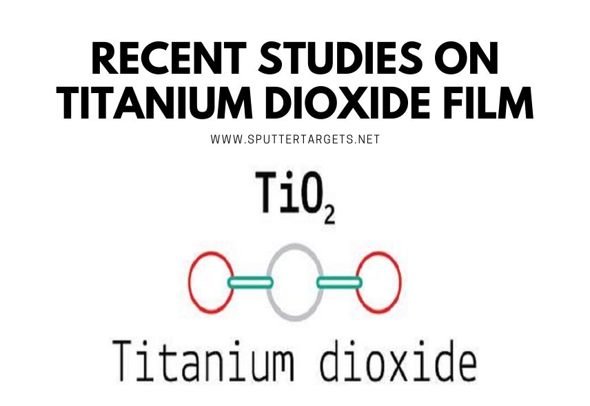
Titanium dioxide (TiO2) is a hard and chemically resistant oxide of titanium. Using TiO2 sputtering target can obtain good quality titanium dioxide films, which have been widely used in various applications due to their multiple interesting properties. The first half of this passage introduces some of the properties and applications of titanium oxide film, and the latter...Continue Reading