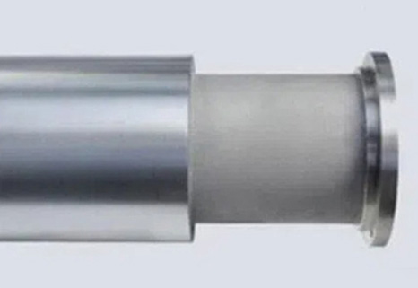
Ever wondered what makes semiconductor devices work like magic? Well, the answer lies in the thin films that coat them, and one of these processes is the rotary metal target. These cylindrical, rotating forms of metal (like tantalum, niobium, and molybdenum) are used in sputtering, a key process in semiconductor manufacturing. If you’re involved in purchasing...Continue Reading
Introduction Hexagonal boron nitride (hBN) is an extremely hot research area within materials and nanotechnology. It possesses remarkable thermal stability, electrical insulation property, and high thermal conductivity, thereby making this material most suitable for various applications in electronic devices, energy storage, and optoelectronic systems. Chemical vapor deposition (CVD) technology is simple, economical and environmentally friendly. It...Continue Reading
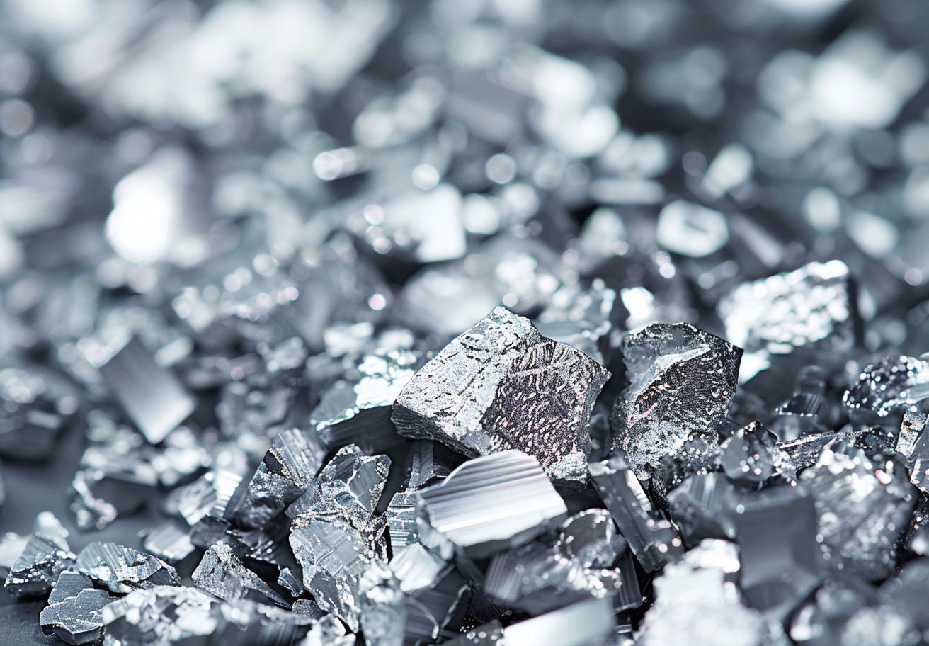
Thin film coating materials play a crucial role in modern industries and technological fields, with widespread applications in electronics, optics, energy, biomedicine, and more. Understanding the classification of thin film materials, specific materials, deposition methods, and their applications helps in making optimal choices and optimizing processes in practical applications. This guide delves into the various...Continue Reading
I. Introduction High-entropy alloys (HEAs) represent a paradigm shift in alloy design. Unlike traditional alloys that rely on a dominant elemental component, HEAs are composed of five or more principal elements in near-equiatomic or equimolar ratios. This unique composition results in high-entropy solid solutions with superior properties not achievable by conventional alloys. The concept of...Continue Reading
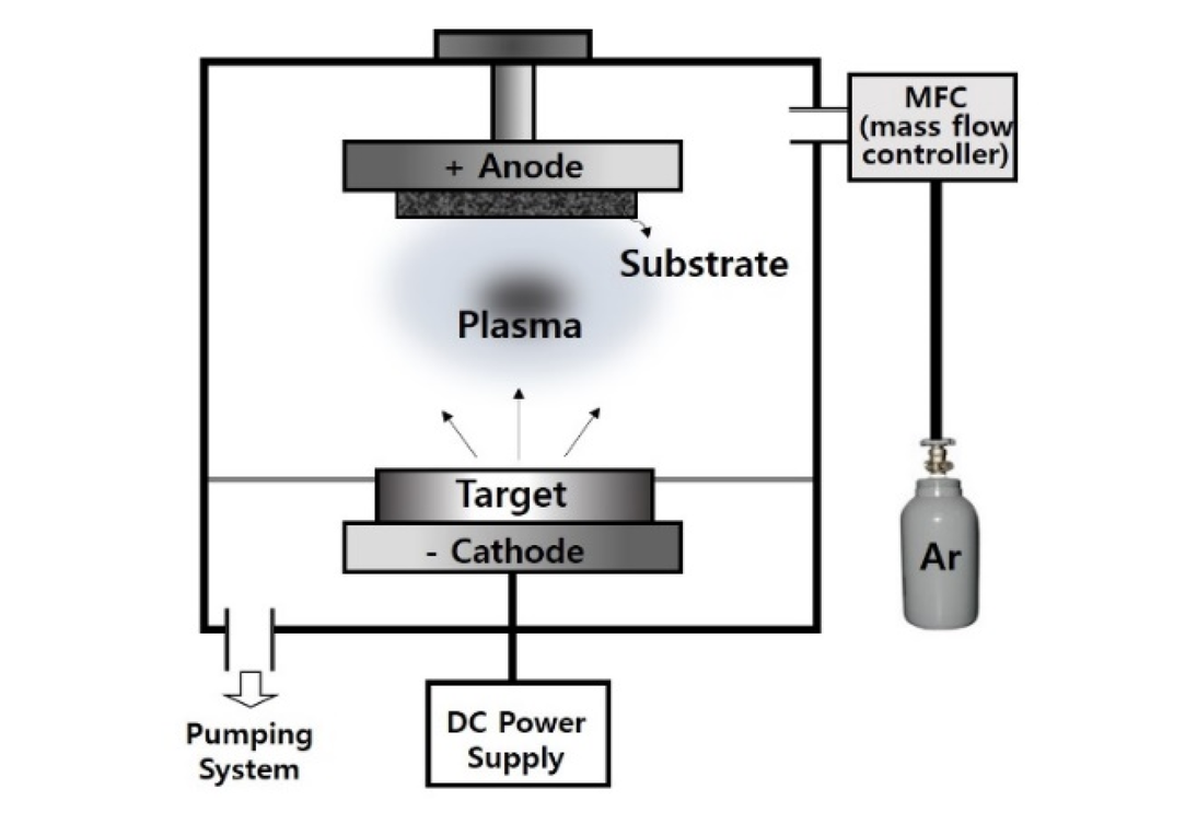
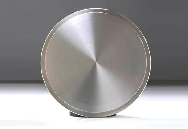
Introduction Background of Sputtering Technology Thin film deposition is a cornerstone in the fabrication of modern technological devices. From electronic components to optical coatings, the demand for high-quality thin films has surged, driving advancements in deposition techniques. Among these, sputtering has emerged as a versatile and reliable method, offering precise control over film composition and...Continue Reading
Introduction Sputtering is a pivotal technique in the fabrication of thin films, widely utilized in industries ranging from semiconductor manufacturing to optics. Its ability to deposit uniform and high-purity coatings makes it indispensable for producing components with stringent performance requirements. Within the sputtering apparatus, backing plates serve as essential components that influence the efficiency and...Continue Reading
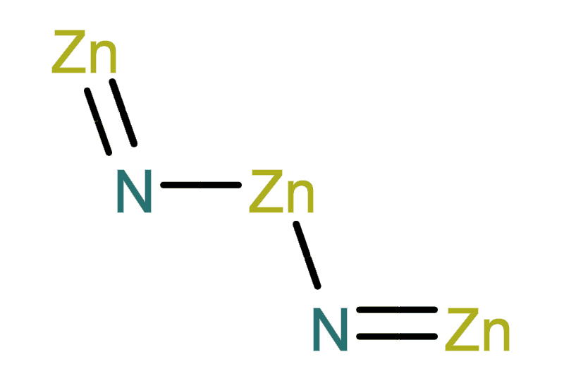
1. Introduction In the rapidly evolving landscape of materials science, the pursuit of novel compounds with superior properties is paramount for advancing various technological applications. Zinc Nitride (Zn₃N₂) has garnered significant attention due to its unique combination of physical and chemical attributes. This compound stands out for its potential applications in electronics, optoelectronics, and as...Continue Reading
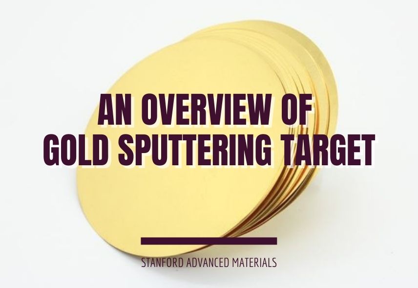
Since ancient times, gold has been revered as a highly valuable material. From making jewelry to cookware and industrial materials, gold has proven to be very useful and precious to man, particularly because of its high malleability, ductility, and lustrous nature. Gold is one of the most precious metals known to man, and it has...Continue Reading
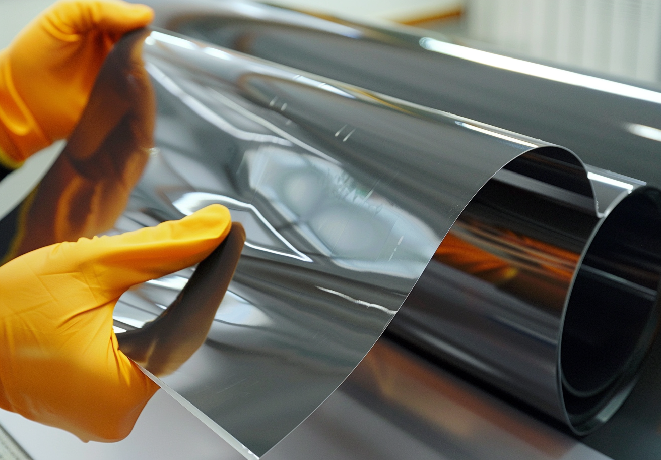
Physical Vapor Deposition (PVD) is a widely used technique in various industries, such as electronics, optics, and materials science. It is crucial for depositing thin films onto substrates, which are essential in the manufacturing of components like semiconductors, mirrors, and solar panels. The quality, thickness, adhesion, and performance of the thin film depend largely on...Continue Reading