Chemical Formula: NdB6
Catalog Number: ST0333
CAS Number: 12045-64-6
Purity: 99.50%
Shape: Discs, Plates, Column Targets, Step Targets, Custom-made
The neodymium boride selenide sputtering target is available in various forms, purities, sizes, and prices. Stanford Advanced Materials (SAM) offers high-quality neodymium boride sputter targets at the most competitive prices.
Neodymium boride sputtering target is a type of boride ceramic sputtering target composed of Neodymium and Boron.
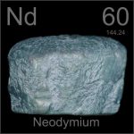
 Neodymium is a chemical element originated from the Greek ‘neos didymos’ meaning new twin. It was first mentioned in 1885 and observed by A. von Welsbach. “Nd” is the canonical chemical symbol of neodymium. Its atomic number in the periodic table of elements is 60 with location at Period 6 and Group 3, belonging to the f-block. The relative atomic mass of neodymium is 144.242(3) Dalton, the number in the brackets indicating the uncertainty.
Related Product: Neodymium Sputtering Target
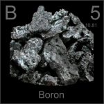
 Boron is a chemical element originated from the Arabic ‘buraq’, which was the name for borax. It was first mentioned in 1808 and observed by L. Gay-Lussac and L.J. Thénard. The isolation was later accomplished and announced by H. Davy. “B” is the canonical chemical symbol of boron. Its atomic number in the periodic table of elements is 5 with location at Period 2 and Group 13, belonging to the p-block. The relative atomic mass of boron is 10.811(7) Dalton, the number in the brackets indicating the uncertainty.
Related Product: Boride Ceramic Sputtering Target
Our neodymium boride sputtering target is carefully packaged in the plastic vacuum bag to prevent damage during storage and transportation and to preserve the quality of our products in their original condition. Also, the COA of the raw material would be packaged with the product.
SAM’s neodymium boride sputtering targets are available in various forms, purities, sizes, and prices. We specialize in producing high purity film coating materials with the highest possible density and smallest possible average grain sizes for use in semiconductor, chemical vapor deposition (CVD) and physical vapor deposition (PVD) display and optical applications. Get an inquiry right now.
Submit your review | |
1 2 3 4 5 | |
Submit Cancel | |